Composite Molded Body of Metal Member and Molded Resin Member, and Surface Processing Method of Metal Member
a technology of molded body and metal member, which is applied in the direction of record information storage, nuclear engineering, railway components, etc., can solve the problems of increased production time, high cost, and inability to form roughened surfaces without substantial practical problems, and achieves short manufacturing time, simple manufacturing step, and inexpensive surface processing technique
- Summary
- Abstract
- Description
- Claims
- Application Information
AI Technical Summary
Benefits of technology
Problems solved by technology
Method used
Image
Examples
first embodiment
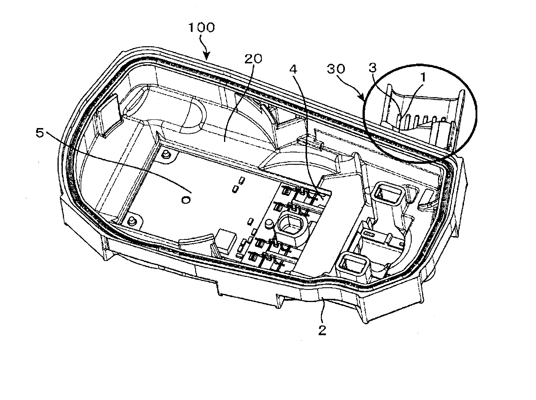
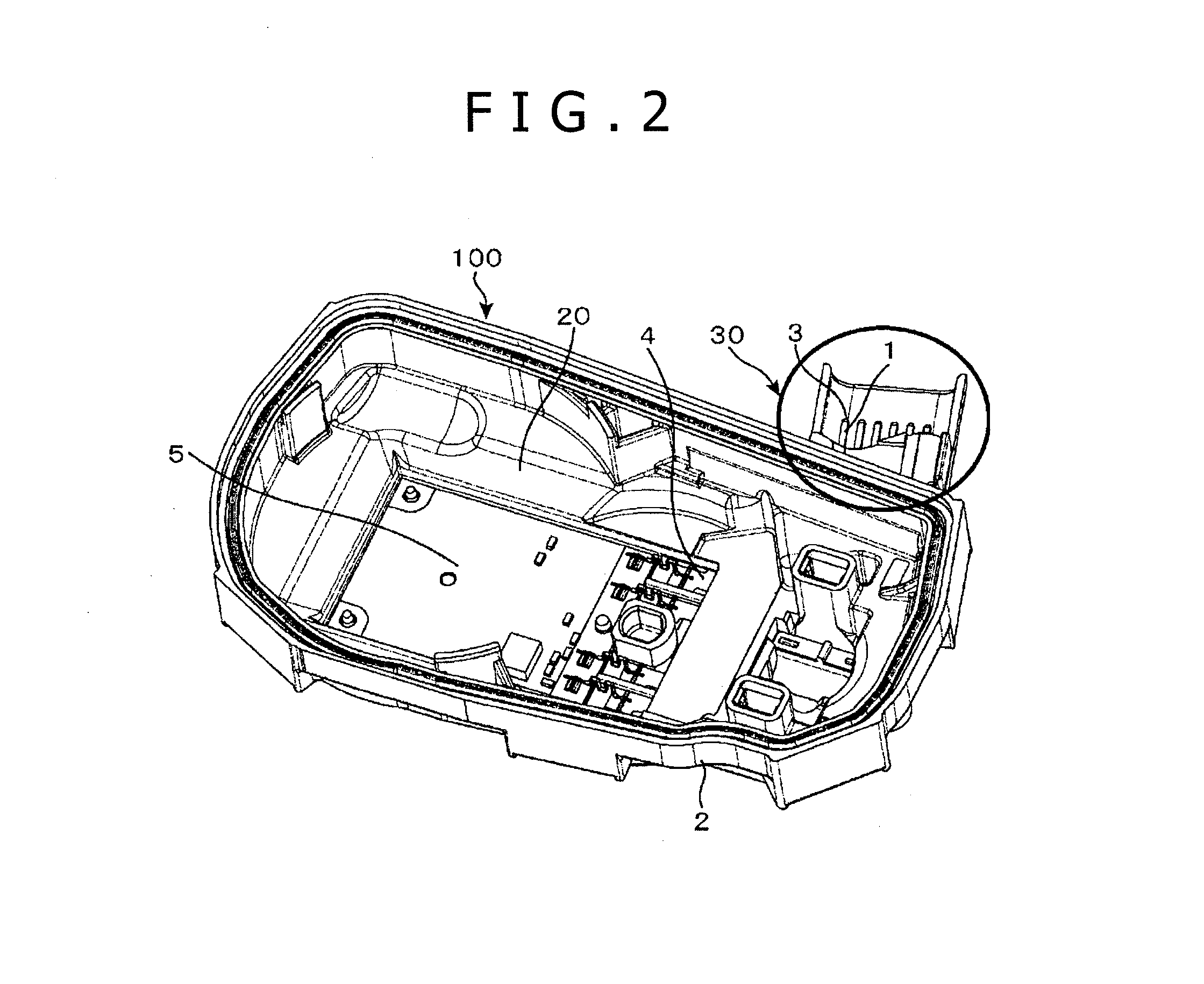
[0042]FIG. 2 shows an appearance of a sensor cover to which the invention is applied, and a connector portion partially broken.
[0043]In FIG. 2, a sensor cover 100 has a connector 30 forming an electric connection portion. The connector 30 has a plurality of metal terminals 1 comprising a copper type alloy material as a metal member which is insert molded to a casing resin portion 2. The casing resin portion 2 as a resin member forms the sensor cover 100. The casing resin portion 2 is formed of a thermoplastic resin PBT (polybutylene terephthalate). The metal terminal 1 is exposed at one end 3 to the outer space of the casing resin portion 2 (space in the connector 30 formed by the casing resin portion 2), and exposed at the other end 4 in a space inside the cover formed by the casing resin portion 2.
[0044]An electronic circuit substrate 5 is fixed to the inner wall surface of the sensor cover 100 formed of the casing resin portion 2. As shown in FIG. 3, the other end 4 of the metal ...
second embodiment
[0081]While the processing of roughening the surface to a metal member having a single plane shape was described as an example, the configuration of the metal material or part is not restricted thereto.
[0082]In the method of melting the surface of a metal by the irradiation of a high density energy beam such as a laser beam or an electron beam, it is necessary to concentrate the energy to a micro region. Accordingly, with the view point of the productivity, it can be said that a single plane is advantageous as the form of a work.
[0083]However, as shown in FIGS. 10A and 10B, a roughened surface portion 14 formed on the surface of a metal member 21 according to the invention has a plurality of grooves 141. In addition, a solidified portion of a metal splash comprising gangue-like prominent portions or prominent portions each having a constriction with a spherical nodule at the top end was formed on the surface of the grooves and the surface of the metal member 21 between the adjacent ...
embodiment 1
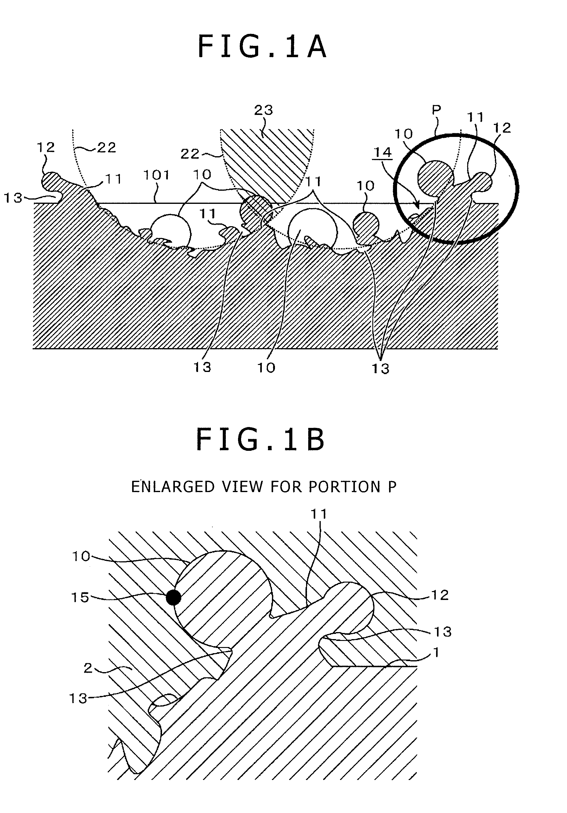
[0107]In a surface processing method of a metal material or a part, a metal surface has a crater-like intricate indent shape formed by melting and scattering of the metal surface by irradiation of a high density energy beam such as a laser beam or an electron beam. The metal surface has gangue-like prominent portions formed by melting and scattering of the metal surface, a spherical metal splash formed at the top end of the prominent portion, and a surface roughened shape where particulate sputtering caused upon fabrication is adhered securely by using the irradiation condition that the crater-like indent fabrication provides a partially overlapped region. The roughened surface shape comprises a joined shape of providing a strong adhesion with a different material.
PUM
| Property | Measurement | Unit |
|---|---|---|
| grain size | aaaaa | aaaaa |
| grain size | aaaaa | aaaaa |
| diameter | aaaaa | aaaaa |
Abstract
Description
Claims
Application Information


