Group iii nitride semiconductor light emitting diode

a semiconductor light-emitting diode and nitride technology, applied in the direction of basic electric elements, electrical equipment, semiconductor devices, etc., can solve the problems of decaying internal quantum efficiency, increase threshold voltage, increase the probability of electron-hole overlap, effect of increasing output power

Inactive Publication Date: 2013-04-11
SOUTHERN TAIWAN UNIVERSITY OF TECHNOLOGY
View PDF4 Cites 2 Cited by
  • Summary
  • Abstract
  • Description
  • Claims
  • Application Information

AI Technical Summary

Benefits of technology

0001] of a hexagonal wurtzite crystal structure formed on the light emitting diode. As a result, the electric field induced by both spontaneous polarization and piezoelectric polarization is parallel to the direction from the f...

Problems solved by technology

Furthermore, the semiconductor light emitting diode suffers from a efficiency droop at higher current densities, resulting in intern...

Method used


Image

  • Group iii nitride semiconductor light emitting diode
  • Group iii nitride semiconductor light emitting diode
  • Group iii nitride semiconductor light emitting diode

Examples


Embodiment Construction

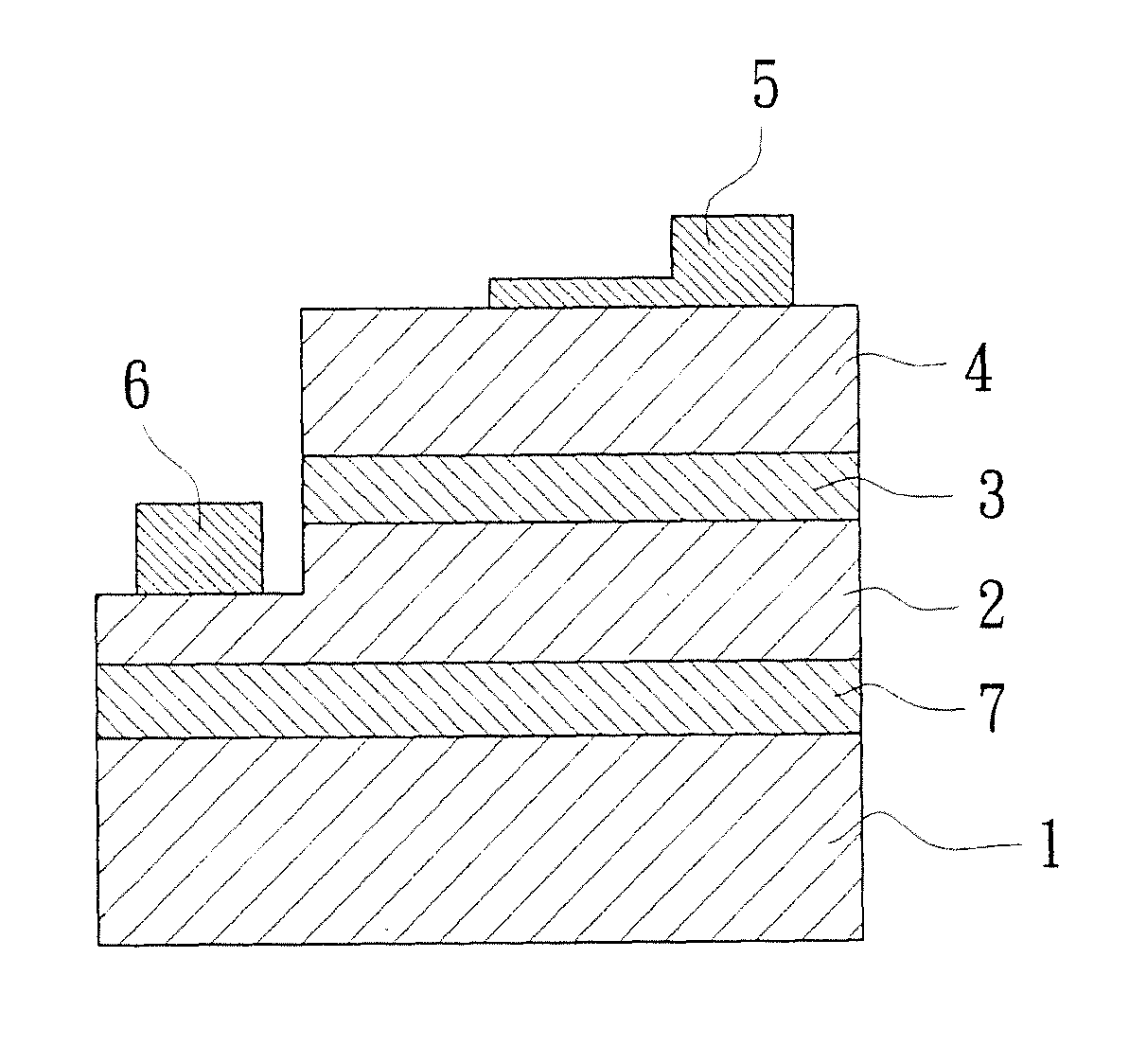
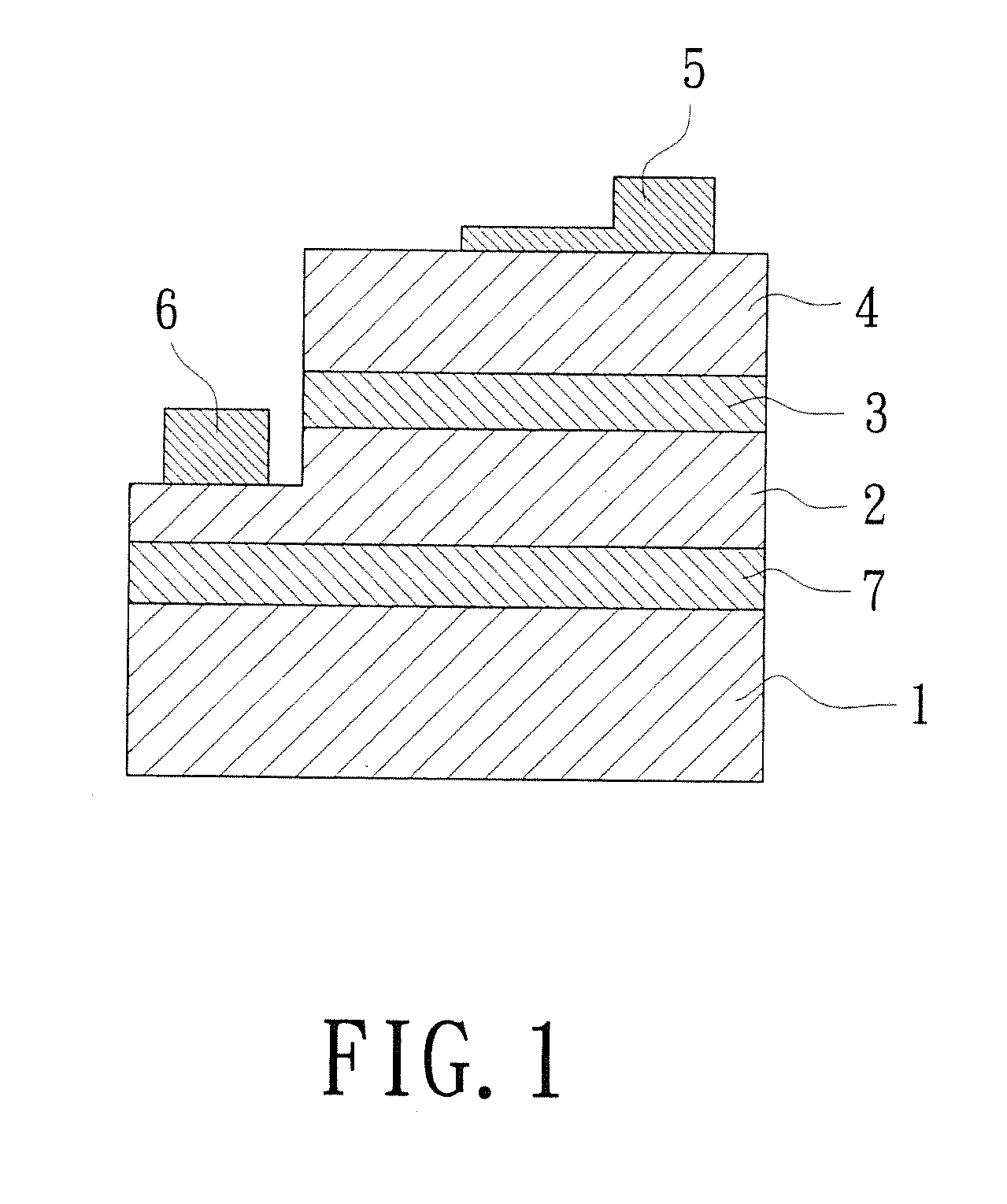
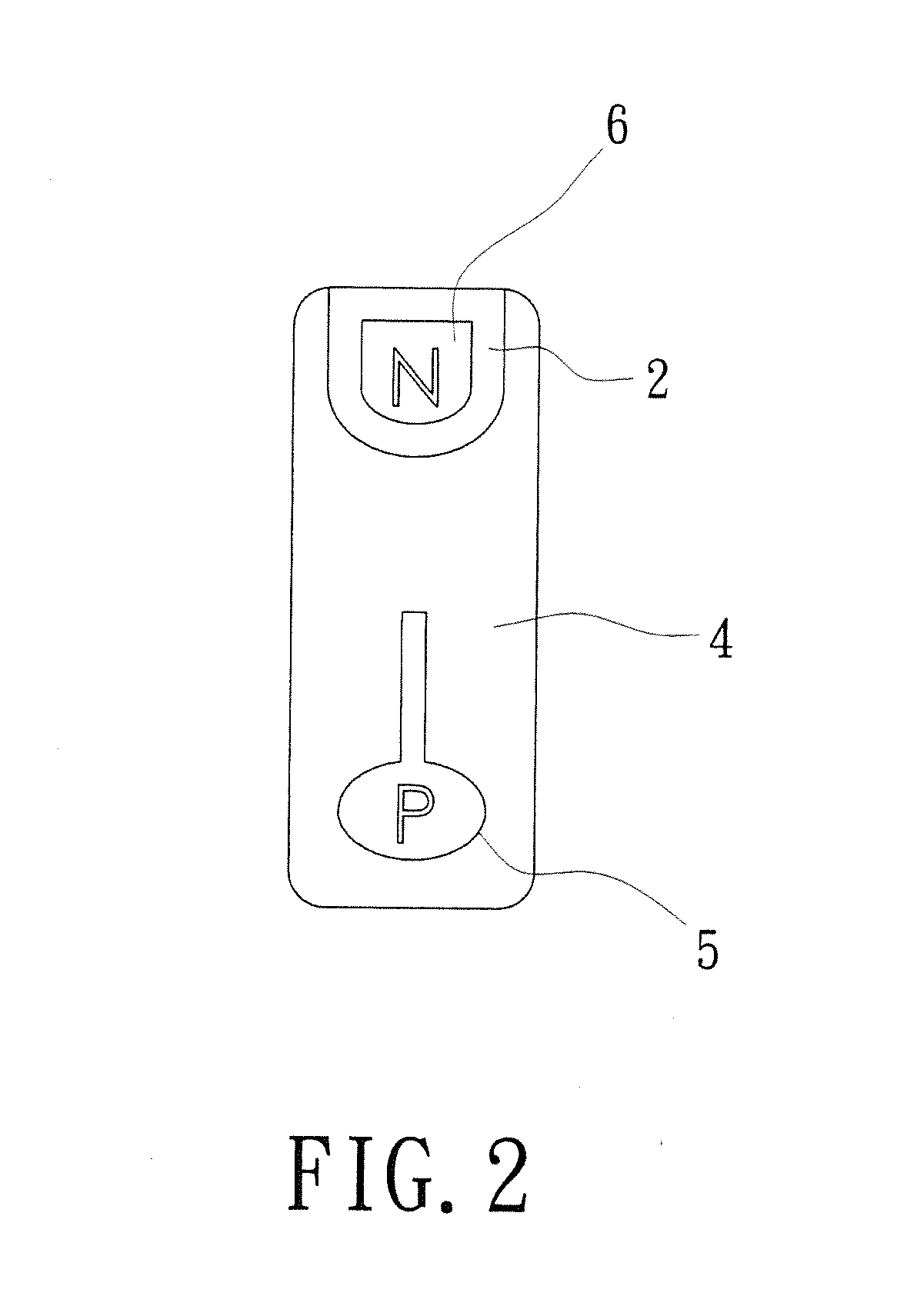
[0016]Referring to FIGS. 1, 2, and 3, a preferred embodiment of the group III nitride semiconductor light emitting diode in accordance with the present invention is revealed, which mainly comprising a substrate 1 for epitaxy growth of a hexagonal wurtzite crystal structure and a layered structure formed on the substrate 1. The layered structure is formed successively with a n-type semiconductor layer 2, a light emitting layer 3 and a p-type semiconductor layer 4. Still, a first electrode metal pad 5 is formed on the p-type semiconductor layer 4 and a second electrode metal pad 6 on the n-type semiconductor layer 2. The n-type semiconductor layer 2, the light emitting layer 3 and the p-type semiconductor layer 4 are all composed of group III nitrides, and a direction from the first electrode metal pad 5 to the second electrode metal pad 6 is the same with the direction of C-axis [0001 ] of the hexagonal wurtzite crystal structure. The first electrode metal pad 5 is a p-type electrode...


PUM


Abstract

A group III nitride semiconductor light emitting diode is revealed. A layered structure composed of group III nitrides is formed on the substrate through epitaxy growth of a hexagonal wurtzite crystal structure. The layered structure includes a n-type semiconductor layer, a light emitting layer on the n-type semiconductor layer, and a p-type semiconductor layer on the light emitting layer. A first electrode metal pad is formed on the p-type semiconductor layer and a second electrode metal pad on the n-type semiconductor layer. A direction from the first electrode metal pad to the second electrode metal pad is the same with that of C-axis [0001] of the hexagonal wurtzite crystal structure so as to speed up the movement of electron-hole and improve the combination efficiency of electron-hole by the electric field along the direction of C-axis [0001] in the hexagonal wurtzite crystal structure.

Description

BACKGROUND OF THE INVENTION[0001]1. Field of the Invention[0002]The present invention relates to a group III nitride semiconductor light emitting diode (LED), especially to a light emitting diode having a substrate and a layered structure formed on the substrate, wherein the direction from the first electrode metal pad to the second electrode metal pad is the same with that of C-axis [0001] of a hexagonal wurtzite crystal structure formed on the light emitting diode, so as to result in a polarization direction parallel to directions of the first and second electrode metal pads to increase the electron-hole combination efficiency, and further to enhance the output power of the light emitting diode.[0003]2. Description of Related Art[0004]In recent years, nitride-based semiconductor light emitting diodes (LEDs) can be made with small components in an environmental manner to reduce mercury pollutions and show a high luminous efficiency, a long lifetime or the like as advantages, so the...

Claims


Application Information

Patent Timeline
IPC IPC(8): H01L33/02H01L33/62
CPCH01L33/32H01L33/16
Inventor CHIOU, YU-ZUNG
Owner SOUTHERN TAIWAN UNIVERSITY OF TECHNOLOGY
Why Eureka
Try Eureka