Solid-state image sensor and manufacturing method thereof, and camera

manufacturing method technology, applied in the field of solid-state image sensors and manufacturing methods thereof, can solve the problems of insufficient water supply to each photoelectric conversion portion, inability to obtain a solid-state image sensor with a low dark current, and insufficient termination of dangling bonds, so as to reduce the dark current of a solid-state image sensor

Inactive Publication Date: 2013-04-11
CANON KK
View PDF4 Cites 6 Cited by
  • Summary
  • Abstract
  • Description
  • Claims
  • Application Information

AI Technical Summary

Benefits of technology

[0007]The present invention provides a technique which is advantageous to reduce a dark current of a solid-state image sensor.

Problems solved by technology

When a pixel is covered by the DCS-SiN, hydrogen supply to each photoelectric conversion portion becomes insufficient, and dangling bonds cannot be sufficiently terminated.
Hence, it is difficult to obtain a solid-state image sensor with a low dark current.
However, with this method, since a substrate suffers plasma damages at the time of formation of the P—SiN, a structure which covers pixels by the P—SiN may increase crystal defects of photoelectric conversion portions.
Hence, this method is disadvantageous to obtain a solid-state image sensor with a low dark current.

Method used


Image

  • Solid-state image sensor and manufacturing method thereof, and camera
  • Solid-state image sensor and manufacturing method thereof, and camera
  • Solid-state image sensor and manufacturing method thereof, and camera

Examples


first embodiment

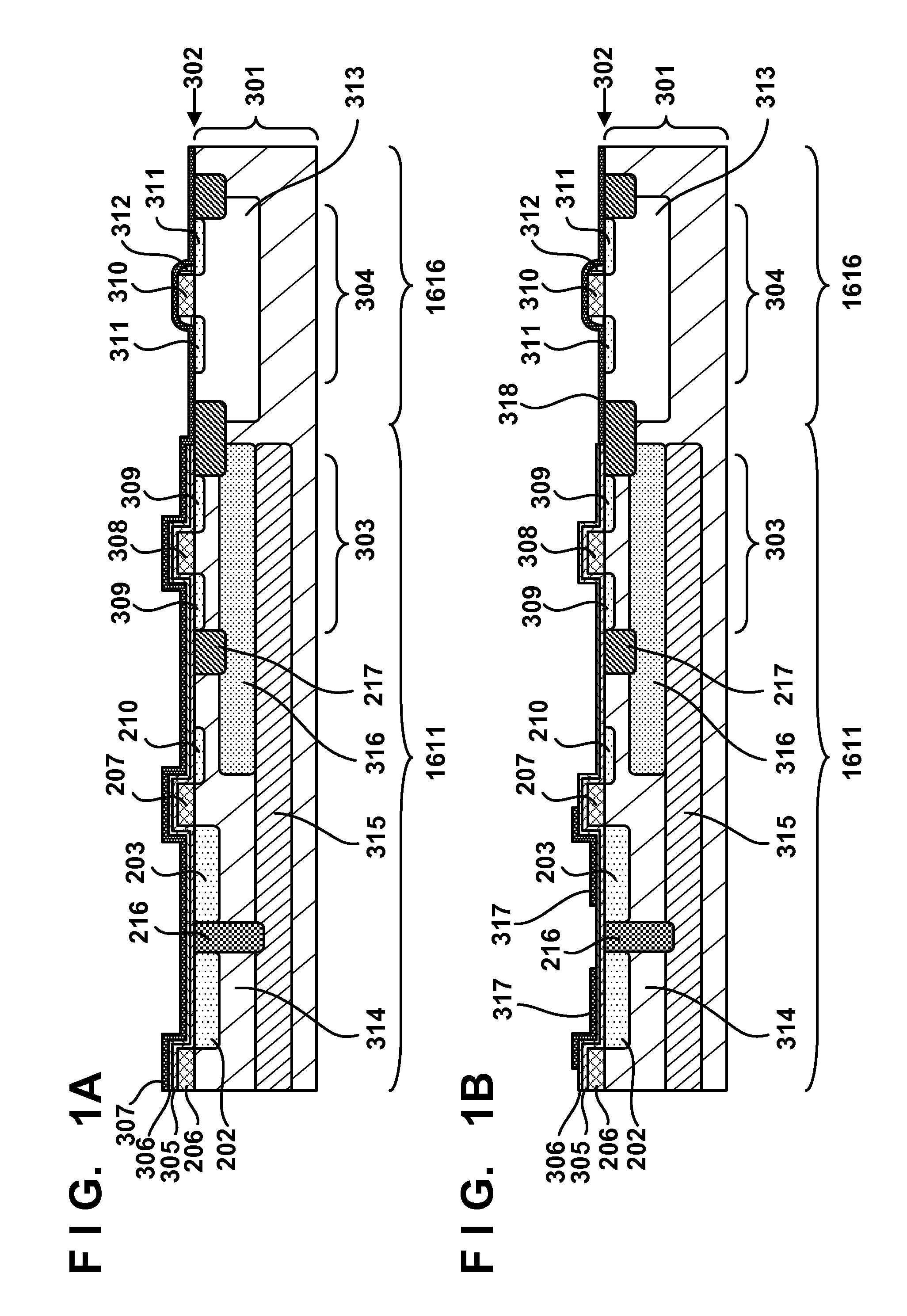
[0022]A manufacturing method of the solid-state image sensor will be described below. In a process shown in FIG. 1A, a semiconductor substrate 301 on which elements such as transistors and photoelectric conversion portions are formed is prepared, and a silicon nitride film 305, silicon oxide film 306, and silicon nitride film 307 are formed as insulation films on a principal face 302 of the semiconductor substrate 301. The semiconductor substrate 301 is typically a silicon substrate, and has the principal face 302. The semiconductor substrate 301 includes n-type semiconductor regions 202 and 203 which respectively configure photoelectric conversion portions (photodiodes), a transistor 303 of the pixel portion 1611, and the transistor 304 of the peripheral circuit portion 1616. The n-type semiconductor regions 202 and 203 function as charge accumulation regions which accumulate charges (electrons in this example). Gate electrodes 206 and 207 of transfer transistors respectively corr...

second embodiment

[0041]In a process shown in FIG. 6A, a structure shown in FIG. 6A is formed by the same method as that described with reference to FIG. 1A. However, in the second embodiment, a silicon nitride film 305 is formed as an HCD-SiN. Next, in a process shown in FIG. 6B, a silicon nitride film 307 formed on a pixel portion 1611 of the pixel portion 1611 and a peripheral circuit portion 1616 is removed to leave a silicon nitride film 318 on the peripheral circuit portion 1616.

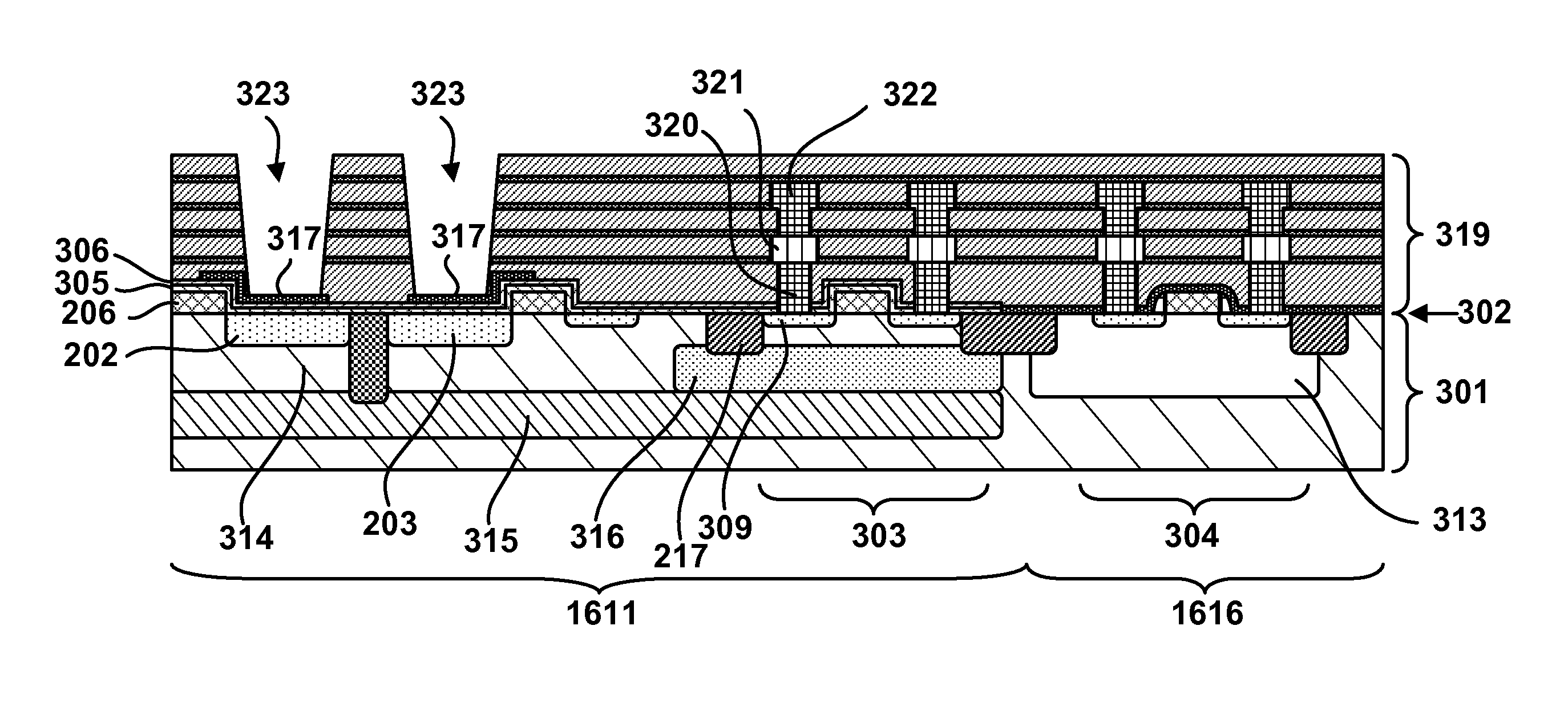
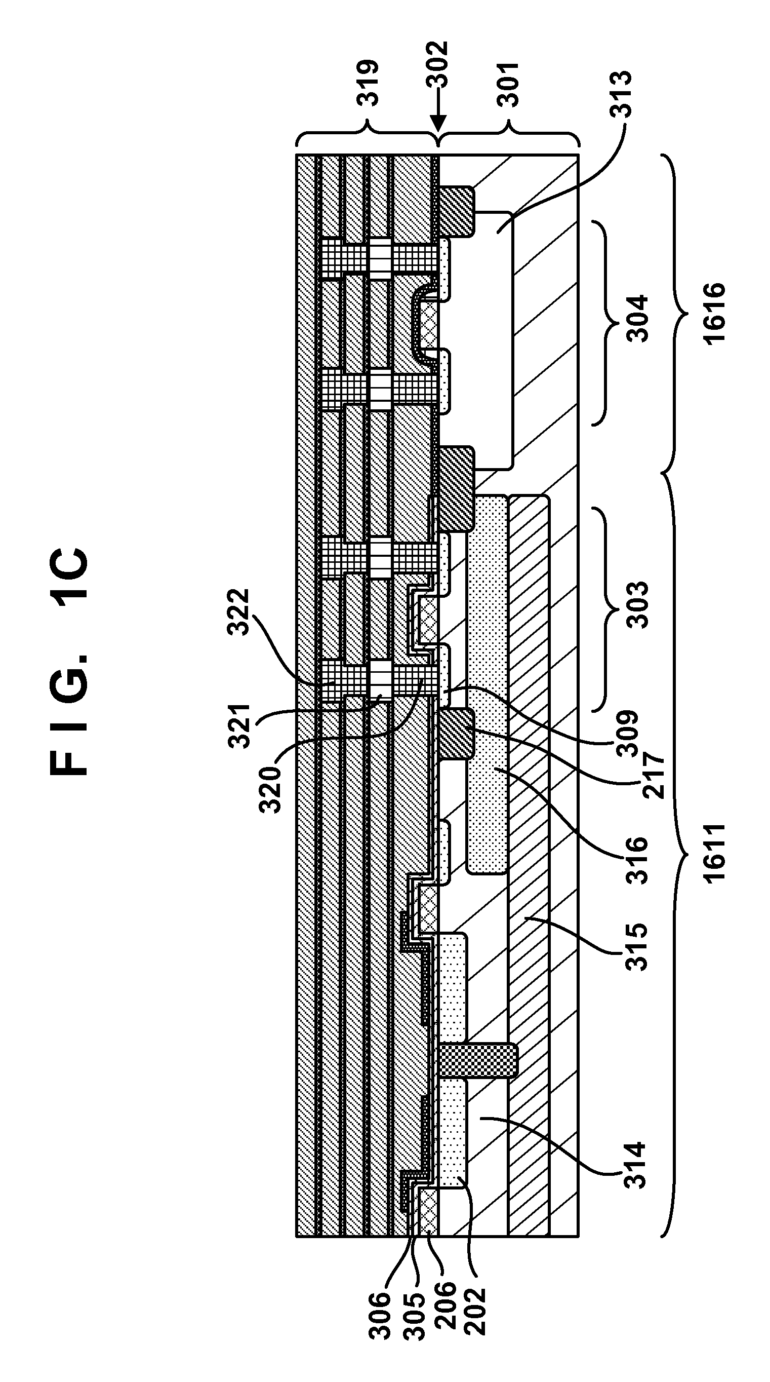
[0042]Next, in a process shown in FIG. 6C, a plurality of interlayer insulation films 319, contact plugs 320, first wiring layers 321, and second wiring layers 322 including a via plug can be formed. The plurality of interlayer insulation films 319 can be configured by alternately stacking silicon oxide films and silicon nitride films. The plurality of interlayer insulation films 319 can be used as claddings of lightguides. The first and second wiring layers 321 and 322 can be formed by a damascene method using, for exa...


PUM

PropertyMeasurementUnit
pressureaaaaaaaaaa
pressureaaaaaaaaaa
thicknessaaaaaaaaaa

Abstract

A method of manufacturing a solid-state image sensor having a photoelectric conversion portion includes forming a silicon nitride film by a low-pressure chemical vapor deposition method using hexachlorodisilane (Si2Cl6) as a material gas such that the silicon nitride film covers at least a part of the photoelectric conversion portion.

Description

BACKGROUND OF THE INVENTION[0001]1. Field of the Invention[0002]The present invention relates to a solid-state image sensor and manufacturing method thereof, and a camera.[0003]2. Description of the Related Art[0004]In recent years, a solid-state image sensor having lightguides for increasing light to be incident on photoelectric conversion portions has been proposed. As described in Japanese Patent Laid-Open No. 2004-207433, a silicon nitride film is formed on a semiconductor substrate, on which photodiodes are formed, by a low-pressure CVD (Chemical Vapor Deposition) method, an interlayer insulation film is formed on the silicon nitride film, and the interlayer insulation film is etched using the silicon nitride film as an etching stopper. Opening portions required to form lightguides are formed by etching the interlayer insulation film. Furthermore, by etching the silicon nitride film via the opening portions, opening portions are also formed in the silicon nitride film. Also, as...

Claims


Application Information

Patent Timeline
Patent Type & Authority Applications(United States)
IPC IPC(8): H01L27/146H04N5/335H01L31/18
CPCH01L27/14627H01L31/103H01L27/14687H01L27/14629
Inventor SHOYAMA, TOSHIHIRO
Owner CANON KK
Why Eureka
Try Eureka