
Semiconductor device

a technology of semiconductors and devices, applied in the field of semiconductor devices, can solve the problems of surge voltage increase, current reduction rate during reverse recovery increase, leakage current increase, etc., and achieve the effect of reducing reverse recovery loss, withstanding voltage increase, and increasing surge voltag

Active Publication Date: 2013-04-18
MITSUBISHI ELECTRIC CORP
View PDF2 Cites 7 Cited by
  • Summary
  • Abstract
  • Description
  • Claims
  • Application Information

AI Technical Summary

Benefits of technology

The present invention seeks to address the problem of reducing reverse recovery loss while improving the withstand voltage of a semiconductor device. By eliminating the use of a short lifetime layer between the N-type drift layer and the P-type anode layer, the number of crystal defects is reduced, resulting in a decrease in current reduction rate during reverse recovery and an increase in withstand voltage. Overall, the present invention provides a semiconductor device that can achieve better performance in terms of withstand voltage and reverse recovery loss suppression.

Problems solved by technology

When the lifetime of the entire device is shortened to reduce reverse recovery loss, the number of crystal defects increases, and this causes a current reduction rate during reverse recovery to increase and causes a surge voltage to increase, which may be a cause of oscillating noise.
Furthermore, the increase in the number of crystal defects causes the leakage current to increase and causes the withstand voltage to decrease.
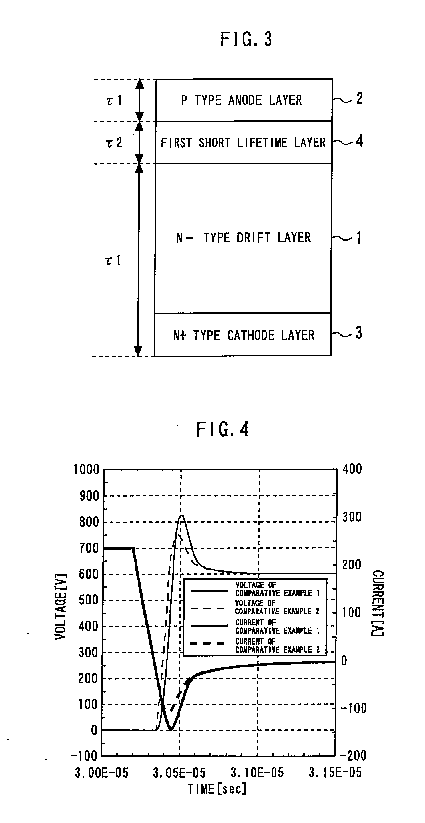
When a short lifetime layer is provided only between the N-type drift layer and the P-type anode layer, a peak value of the reverse recovery current decreases, which provides an advantage that the reverse recovery current reduction rate decreases, but there is also a disadvantage that the withstand voltage decreases and the reverse recovery loss increases.

Method used


Image

  • Semiconductor device
  • Semiconductor device
  • Semiconductor device

Examples


Embodiment Construction

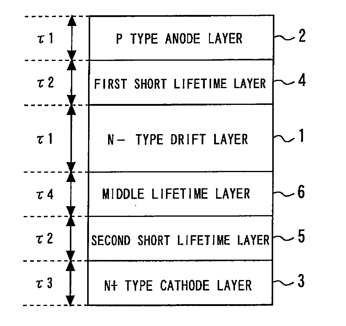
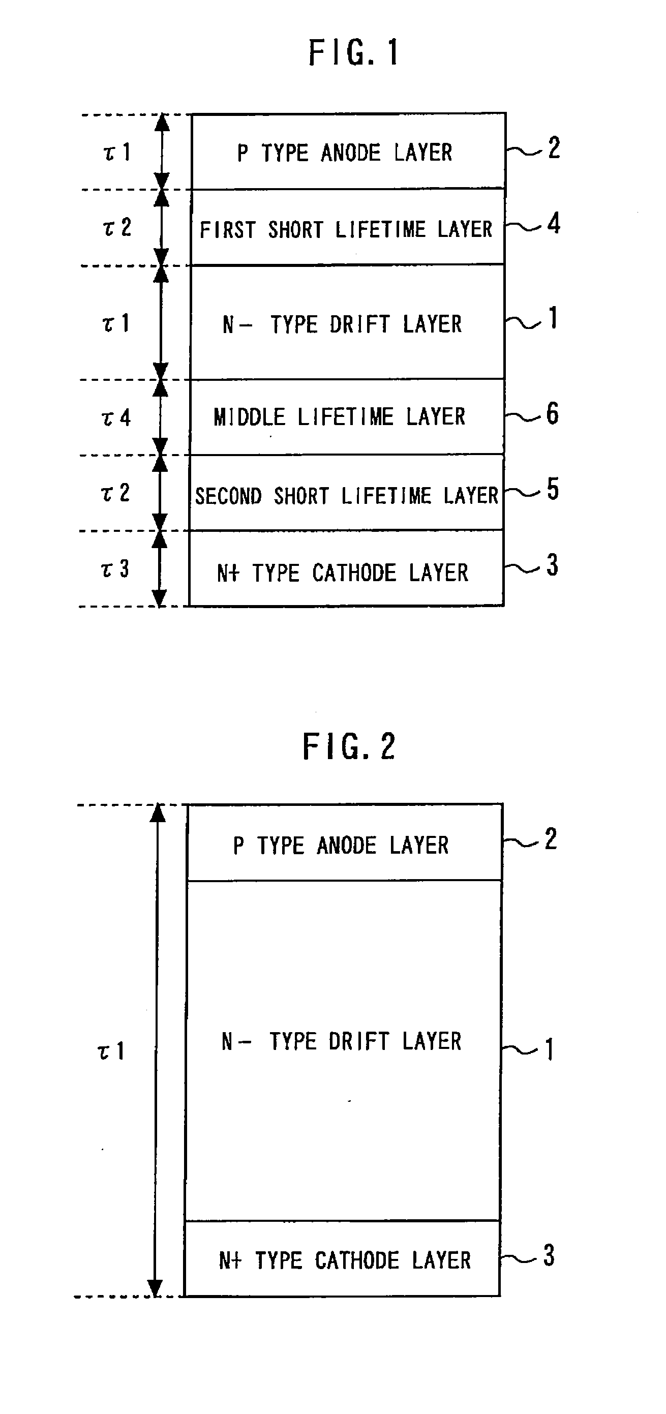
[0021]FIG. 1 is a cross-sectional view illustrating a semiconductor device according to an embodiment of the present invention. A P-type anode layer 2 is provided above an N−-type drift layer 1. An N+-type cathode layer 3 is provided below the N−-type drift layer 1.

[0022]A first short lifetime layer 4 is provided between the N−-type drift layer 1 and the P-type anode layer 2. A second short lifetime layer 5 is provided between the N−-type drift layer 1 and the N+-type cathode layer3. A middle lifetime layer 6 is provided between the N−-type drift layer 1 and the second short lifetime layer 5. The first and second short lifetime layers 4 and 5, and the middle lifetime layer 6 are formed by locally irradiating protons into the N−-type drift layer 1.

[0023]A carrier lifetime τ2 in the first and second short lifetime layers 4 and 5 is shorter than a lifetime τ1 in the N−-type drift layer 1 (τ21). A lifetime τ3 in the N+-type cathode layer 3 is longer than the lifetime τ1 in the N−-type d...


PUM


Abstract

A semiconductor device includes: an N-type drift layer; a P-type anode layer above the N-type drift layer; an N-type cathode layer below the N-type drift layer; a first short lifetime layer between the N-type drift layer and the P-type anode layer; and a second short lifetime layer between the N-type drift layer and the N-type cathode layer. A carrier lifetime in the first and second short lifetime layers is shorter than a carrier lifetime in the N-type drift layer. A carrier lifetime in the N-type cathode layer is longer than the carrier lifetime in the N-type drift layer.

Description

BACKGROUND OF THE INVENTION[0001]1. Field of the Invention[0002]The present invention relates to a diode which is one of devices constituting a power module, and more particularly, to a semiconductor device that can improve a withstand voltage while reducing reverse recovery loss and suppressing a surge voltage.[0003]2. Background Art[0004]Reverse recovery loss, which is an important characteristic of diodes, has relevance to the lifetime of a carrier. When, for example, the number of crystal defects is increased to shorten the lifetime, the reverse recovery loss decreases. Thus, a technique of introducing crystal defects through irradiation of an electron beam and controlling the lifetime of the entire device is used to obtain a diode which has arbitrary reverse recovery loss.[0005]Furthermore, a diode is also proposed in which crystal defects are partially introduced between an N-type drift layer and a P-type anode layer and a short lifetime layer whose carrier has a short lifetim...

Claims


Application Information

Patent Timeline
Patent Type & Authority Applications(United States)
IPC IPC(8): H01L29/02
CPCH01L29/36H01L29/32H01L29/861
Inventor KACHI, TAKAOYOSHIURA, YASUHIROMASUOKA, FUMIHITO
Owner MITSUBISHI ELECTRIC CORP
Learn More