Semiconductor light emitting device and vehicle lamp
a technology of light source, which is applied in the direction of point-like light source, lighting and heating apparatus, transportation and packaging, etc., can solve the problems of difficult to make the brightness distribution completely uniform, color unevenness occurring in mixed light, and intentionally making the brightness distribution over the light emitting surface non-uniform, etc., to reduce the amount of light, improve the efficiency of light from the semiconductor light emitting device, and reduce the effect of chromaticity differen
- Summary
- Abstract
- Description
- Claims
- Application Information
AI Technical Summary
Benefits of technology
Problems solved by technology
Method used
Image
Examples
embodiment 1
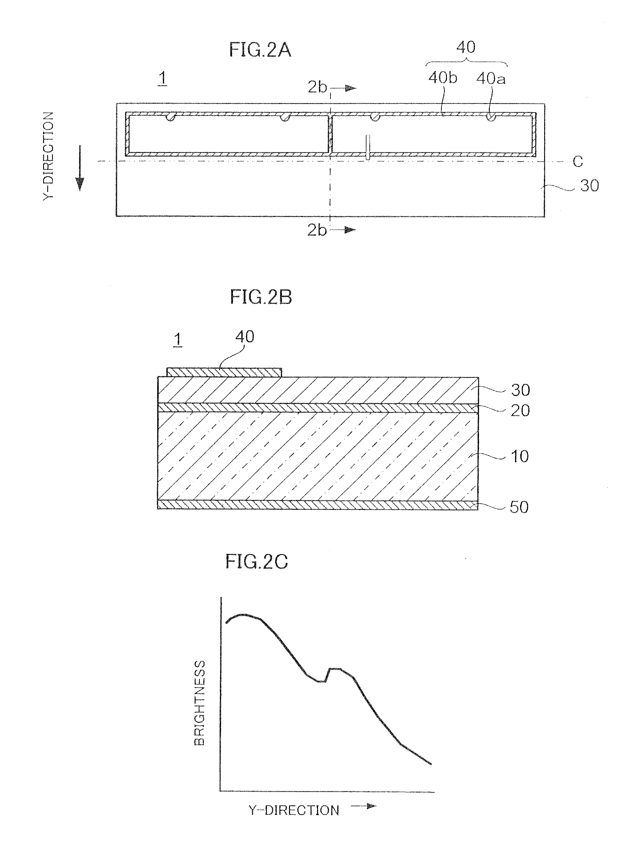
[0049]FIG. 2A is a plan view showing the configuration of a semiconductor light emitting element 1 according to an embodiment of the present invention, and FIG. 2B is a cross-sectional view taken along line 2b-2b in FIG. 2A. FIG. 2C is a graph showing the brightness distribution along the Y-direction in FIG. 2A of the semiconductor light emitting element 1. The semiconductor light emitting element 1 is a so-called thin-film structured light emitting element comprising a semiconductor film 30 and a support substrate 10 bonded together. Also, the semiconductor light emitting element 1 is a so-called vertically-structured light emitting element wherein a p-electrode 20 and an n-electrode 40 are placed opposite each other on opposite sides of the semiconductor film 30.
[0050]The support substrate 10 is made of, e.g., material of higher thermal conductivity (such as silicon or metal) than a growth substrate (not shown) used in the crystal growth of the semiconductor film 30. The p-electro...
embodiment 2
[0053]FIG. 4 is a cross-sectional view showing the structure of a semiconductor light emitting device 2b according to Embodiment 2 of the present invention, which is configured with a wavelength converting layer containing a fluorescent substance and laid over the surface (principal light emitting surface) of the above semiconductor light emitting element 1. The semiconductor light emitting device 2b has three wavelength converting layers 60a, 60b, 60c, which are different in the concentration of a fluorescent substance contained therein, on the surface of the semiconductor light emitting element 1. The three wavelength converting layers 60a, 60b, 60c have the concentrations of the fluorescent substance adjusted correspondingly to the non-uniform brightness distribution at light emission operation of the semiconductor light emitting element 1. Namely, the concentration of the fluorescent substance contained in the wavelength converting layer 60a, which covers the area of the highest...
embodiment 3
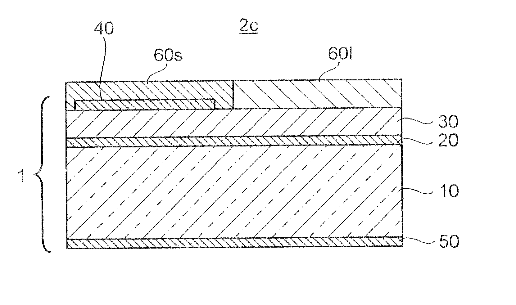
[0054]FIG. 5 is a cross-sectional view showing the structure of a semiconductor light emitting device 2c according to Embodiment 3 of the present invention, which is configured with a wavelength converting layer containing a fluorescent substance and laid over the surface of the above semiconductor light emitting element 1. In the semiconductor light emitting device 2c, wavelength converting layers 60s, 601, which contain fluorescent substances having different dominant wavelengths, are provided on the surface of the semiconductor light emitting element 1.
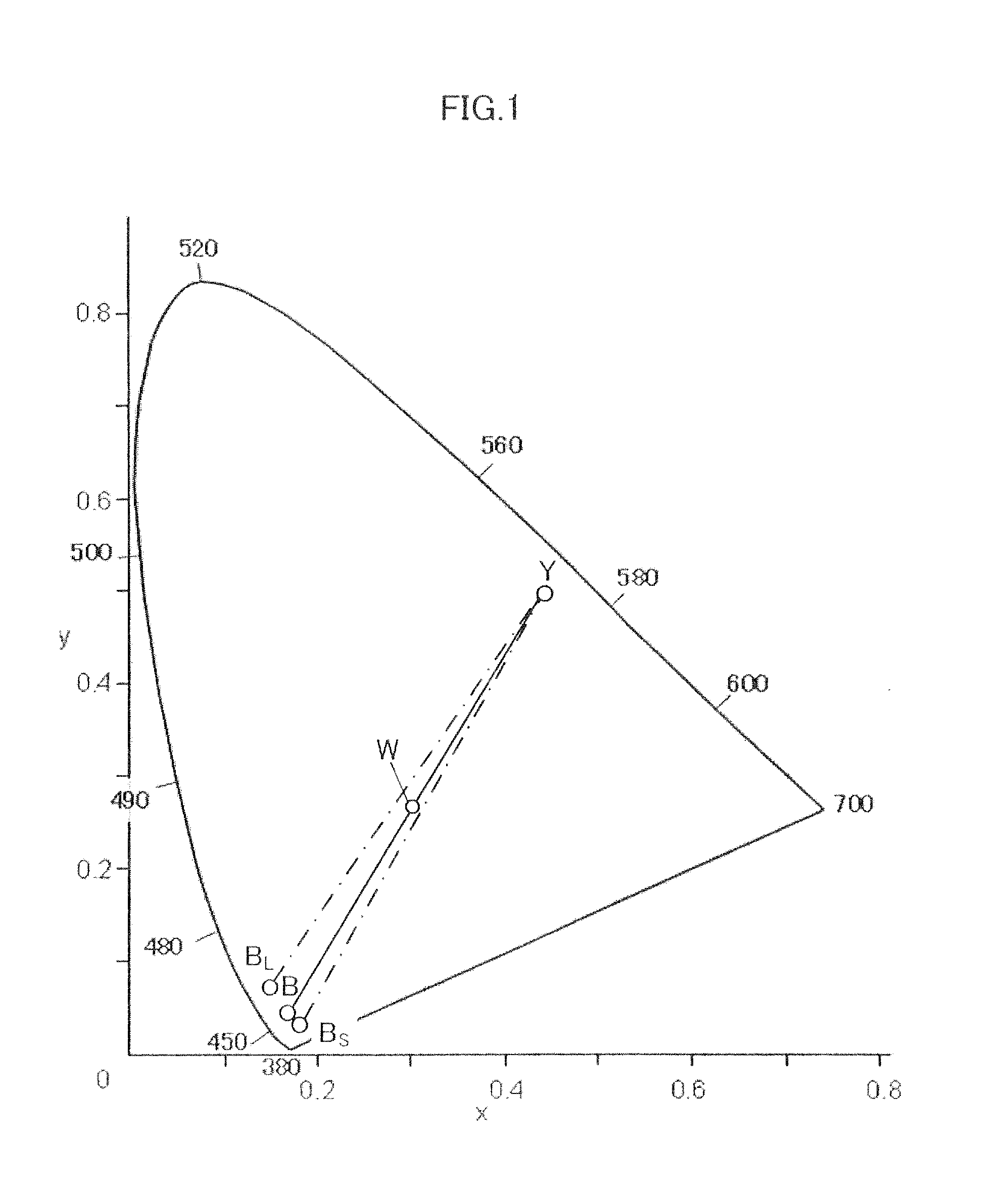
[0055]In the semiconductor light emitting element 1, the current density is high at the area over which the n-electrode 40 extends and low at the area over which the n-electrode 40 does not extend. Hence, the emission wavelength at the area over which the n-electrode 40 extends is shorter than the emission wavelength at the area over which the n-electrode 40 does not extend (blue shift). That is, the semiconductor light emitting el...
PUM
 Abstract
Description
Claims
Application Information
 - R&D
- Intellectual Property
- Life Sciences
- Materials
- Tech Scout
- Unparalleled Data Quality
- Higher Quality Content
- 60% Fewer Hallucinations
Browse by: Latest US Patents, China's latest patents, Technical Efficacy Thesaurus, Application Domain, Technology Topic, Popular Technical Reports.
© 2025 PatSnap. All rights reserved.Legal|Privacy policy|Modern Slavery Act Transparency Statement|Sitemap|About US| Contact US: help@patsnap.com


