Flexible and moldable materials with bi-conductive surfaces

a technology of bi-conductive surfaces and flexible materials, applied in the field of functionalized particle polymer matrix composites, can solve the problems of high noise levels of piezoresistive strips by themselves due to common-mode noise, and the current cost of motion capture rooms and lidar is prohibitively expensive for general and personal use, etc., and achieves the effects of convenient manufacturing, low cost, and convenient us

Inactive Publication Date: 2013-05-02
RGT UNIV OF CALIFORNIA
View PDF4 Cites 7 Cited by
  • Summary
  • Abstract
  • Description
  • Claims
  • Application Information

AI Technical Summary

Benefits of technology

[0013]The construct material can be fabricated using simple, cost-effective, and scalable deposition processes. The material is a composite structure composed of at least two conductive sheets that sandwich a thin polymer insulator layer that are all bonded together at their interfaces. The two conductive sheets are made of conductive particles or semi-conductive particles dispersed through a flexible polymer.
[0017]In an alternative embodiment, the two outer active surfaces can be covered with an outer protective coating that is flexible to improve durability and that will shield and protect the active layers. For example, the outer surface can be a layer of insulating polymer such as used in the center of the laminate construct. This electrically insulative protective layer can not only protect the structural integrity of the conductive layers, the protective layer can also electrically insulate the conductive layers from outside noise or other interference. In another embodiment, only one surface is covered with a protective layer because the laminate is placed on a substrate that protects the bottom active layer.
[0020]The structure of the laminate construct can also be used to create a flexible capacitor. With the ability to tailor the lateral and vertical dimensions of the conductive and insulating layers, the resulting capacitance of the material can be customized for a given application. This may be a complementary technology to the developing field of flexible circuits because of the incorporation of low-cost materials and simple fabrication processes.
[0023]Another aspect of the invention is to provide a system for monitoring changes in surface shape that is portable, inexpensive, durable, and works in many places where traditional shape monitoring techniques would fail.
[0024]Another aspect of the invention is to provide a laminate that is inexpensive, easy to manufacture, durable and adaptable to a wide variety of uses.
[0025]A further aspect of the invention is to provide a bi-conductive sheet and system that is ideally suited to monitoring large-scale surface deformations on surfaces like cloth without excessive wiring or the need for special purpose equipment.

Problems solved by technology

However, motion capture rooms and LIDAR currently are prohibitively expensive for general and personal use.
LIDAR and stereovision have difficulties with handling occlusions due to line-of-sight constraints, absorbing materials, and low-level illumination.
However, piezoresistive strips by themselves appear to suffer from high noise levels due to common-mode noise, potentially stemming from wiring constraints and the triboelectric or electromechanical interaction of the materials.
There are also calibration issues that arise if the strips are directly embedded in cloth due to the difficulty in controlling layer thickness and the interactions that occur between the textile and strain-gauge materials.
One significant difficulty with this strain-gauge approach is that the number of electrodes and attached wires scales linearly with the number of strain gauges.
Unfortunately, highly conductive lines are costly to make both flexible and durable, and processing to add in numerous lines to a sheet can both affect the mechanical bending properties of the surface and substantially drive up manufacturing costs.

Method used


Image

  • Flexible and moldable materials with bi-conductive surfaces
  • Flexible and moldable materials with bi-conductive surfaces
  • Flexible and moldable materials with bi-conductive surfaces

Examples


example 1

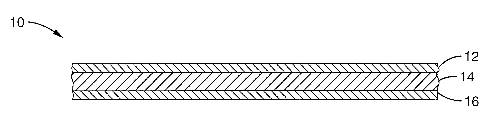
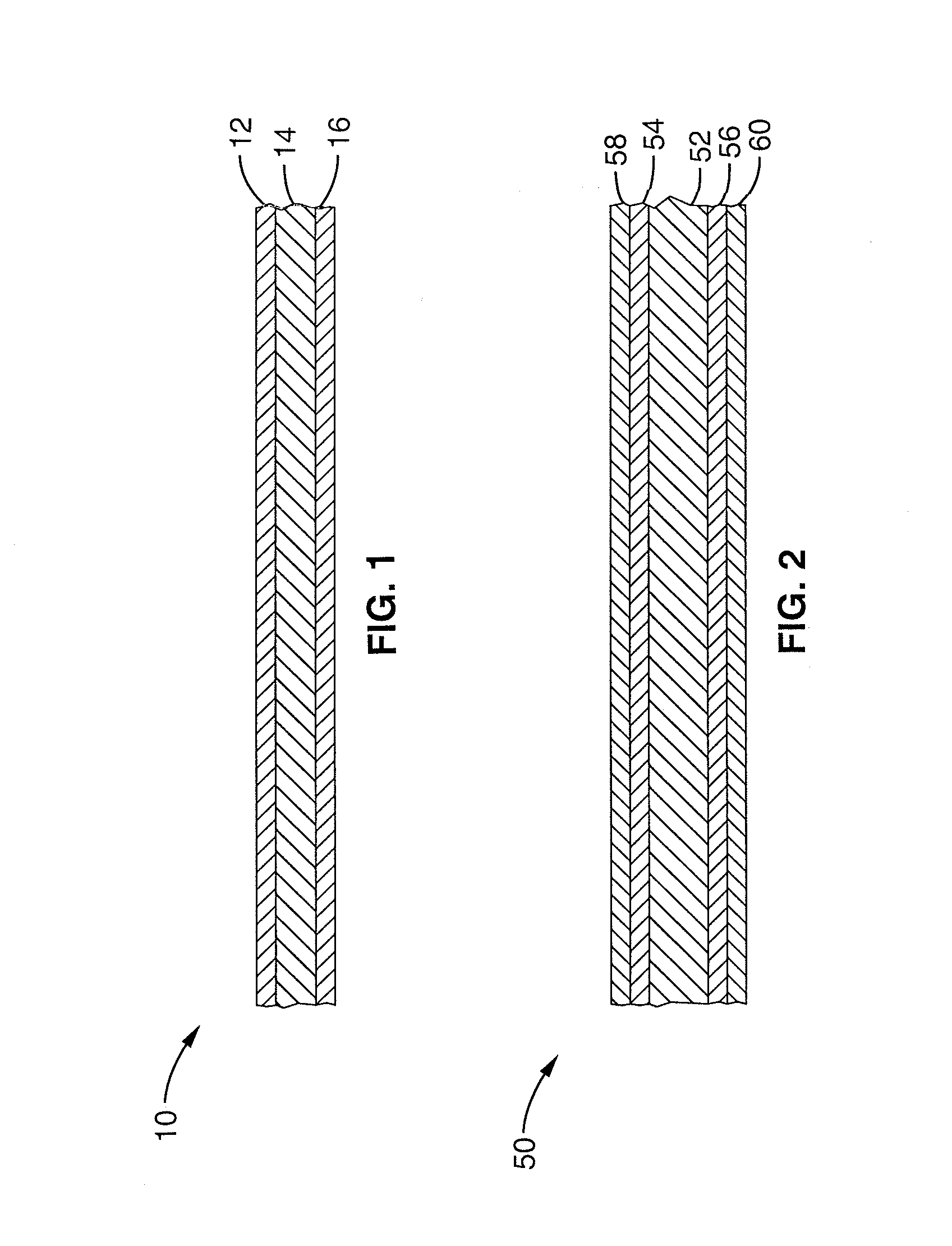
[0046]In order to illustrate the methods for fabrication and the functionality of the resulting bi-conductive material construct, a composite structure composed of two outer sheets of conductive particles dispersed in a flexible polymer sandwiching a thin polymer layer was produced.

[0047]The conductive material layers were produced from 20 grams of poly di-methyl silane (PDMS); 1 gram of PDMS curing agent; 5 grams of Acetylene black (AB) and 57.7 grams of Toluene solvent. In this illustration, the non-conductive center material was produced from 20 grams of poly di-methyl silane (PDMS) and 1 gram of PDMS curing agent.

[0048]A slurry of conductive material was prepared as follows:

[0049]1) PDMS and curing agent were mixed rigorously;

[0050]2) Mixture was de-gased thoroughly so that no trapped air bubbles were visible. This was done by using a light vacuum and allowing the ink to sit idle for more than 15 minutes;

[0051]3) Acetylene black was added in 0.5 gram increments and mixed;

[0052]4...

example 2

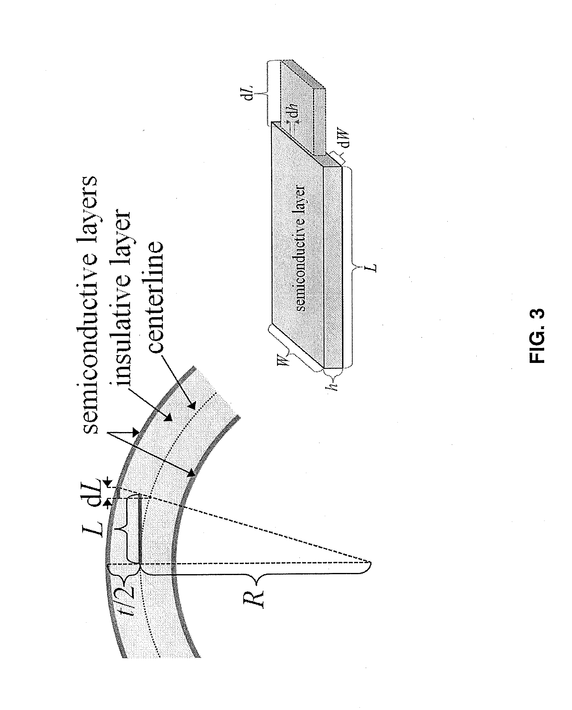
[0063]The flexible bi-conductive material of the present invention can be used in a variety of fields including shielding, flexible capacitors, and strain gauges. As an illustration of a strain gauge configuration, a semiconductor-insulator-semiconductor composite structure with electrodes attached at the boundary was produced and tested.

[0064]The electrical properties of the material were sampled by applying currents and measuring resulting voltages at the boundary electrodes. The piezoresistive and geometry changes of the semiconductor layers results in resistance variations across the surface according to local curvature. Through sufficient sampling, a system of equations can be solved for the interior curvature properties. The local curvature data is integrated to yield an approximation of the surface shape.

[0065]The system preferably contains a single laminate sheet to reduce the requirements on wiring. While a single strain-gauge layer is sufficient for determining purely stre...


PUM

PropertyMeasurementUnit
thicknessesaaaaaaaaaa
thicknessaaaaaaaaaa
thicknessaaaaaaaaaa

Abstract

A flexible, moldable material is provided with bi-conductive surfaces that can be fabricated using simple, cost-effective, and scalable deposition processes. The material is a composite structure composed of two conductive or semi-conductive sheets sandwiching a thin polymer insulator, all bonded together at their interfaces. The two functionalized sheets are made of conductive or semi-conductive particles dispersed through a flexible polymer. In one embodiment, a protective coating over the outer conductive sheets is applied to improve the durability of the composite structure. The material can be patterned into custom shapes and patterns with sizes ranging from meso-scale (millimeters) to macro-scale (meters) dimensions. The thicknesses of the components can also be tailored to be thin, such as a few hundred microns, yet the material maintains very good durability.

Description

CROSS-REFERENCE TO RELATED APPLICATIONS[0001]This application a 35 U.S.C. §111(a) continuation of PCT international application number PCT / US2011 / 035039 filed on May 3, 2011, incorporated herein by reference in its entirety, which is a nonprovisional of U.S. provisional patent application Ser. No. 61 / 330,804 filed on May 3, 2010, incorporated herein by reference in its entirety. Priority is claimed to each of the foregoing applications.[0002]The above-referenced PCT international application was published as PCT International Publication No. WO 2011 / 140119 on Nov. 10, 2011 and republished on Mar. 1, 2012, and is incorporated herein by reference in its entirety.STATEMENT REGARDING FEDERALLY SPONSORED RESEARCH OR DEVELOPMENT[0003]Not ApplicableINCORPORATION-BY-REFERENCE OF MATERIAL SUBMITTED ON A COMPACT DISC[0004]Not ApplicableBACKGROUND OF THE INVENTION[0005]1. Field of the Invention[0006]This invention pertains generally to functionalized particle polymer matrix composites, and mor...

Claims


Application Information

Patent Timeline
Patent Type & Authority Applications(United States)
IPC IPC(8): H01B7/04
CPCB32B27/08H01B7/04B32B2457/00B32B27/14B32B27/28B32B27/304B32B27/306B32B27/322B32B2262/103B32B2264/10B32B2264/102B32B2264/105B32B2264/108B32B2307/202B32B2307/206B32B2307/546B32B2307/732B32B2419/00B32B2307/212
Inventor KIRK, ADAMHO, CHRISTINEDE LA FUENTE VORNBROCK, ALEJANDROGARMIRE, DAVID
Owner RGT UNIV OF CALIFORNIA
Why Eureka
Try Eureka