

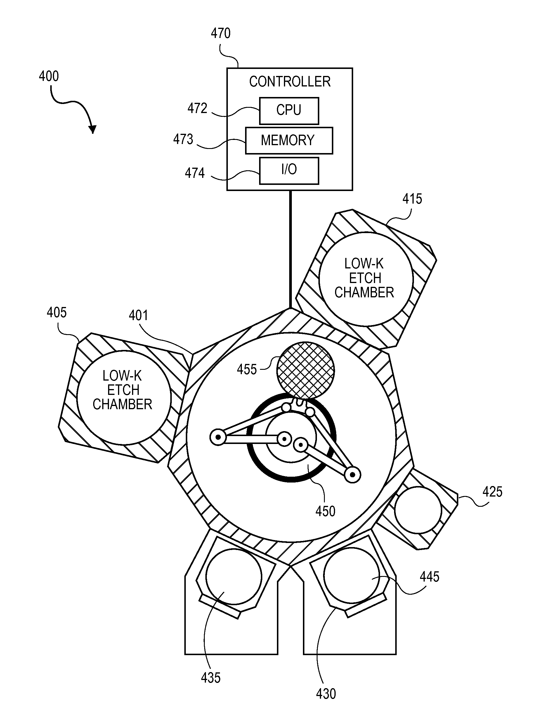
Process chamber for etching low k and other dielectric films
a dielectric film and process chamber technology, applied in the field of microelectronic device processing, can solve problems such as adversely affecting the performance of the devi
- Summary
- Abstract
- Description
- Claims
- Application Information
AI Technical Summary
Benefits of technology
Problems solved by technology
Method used
Image

Examples
Embodiment Construction
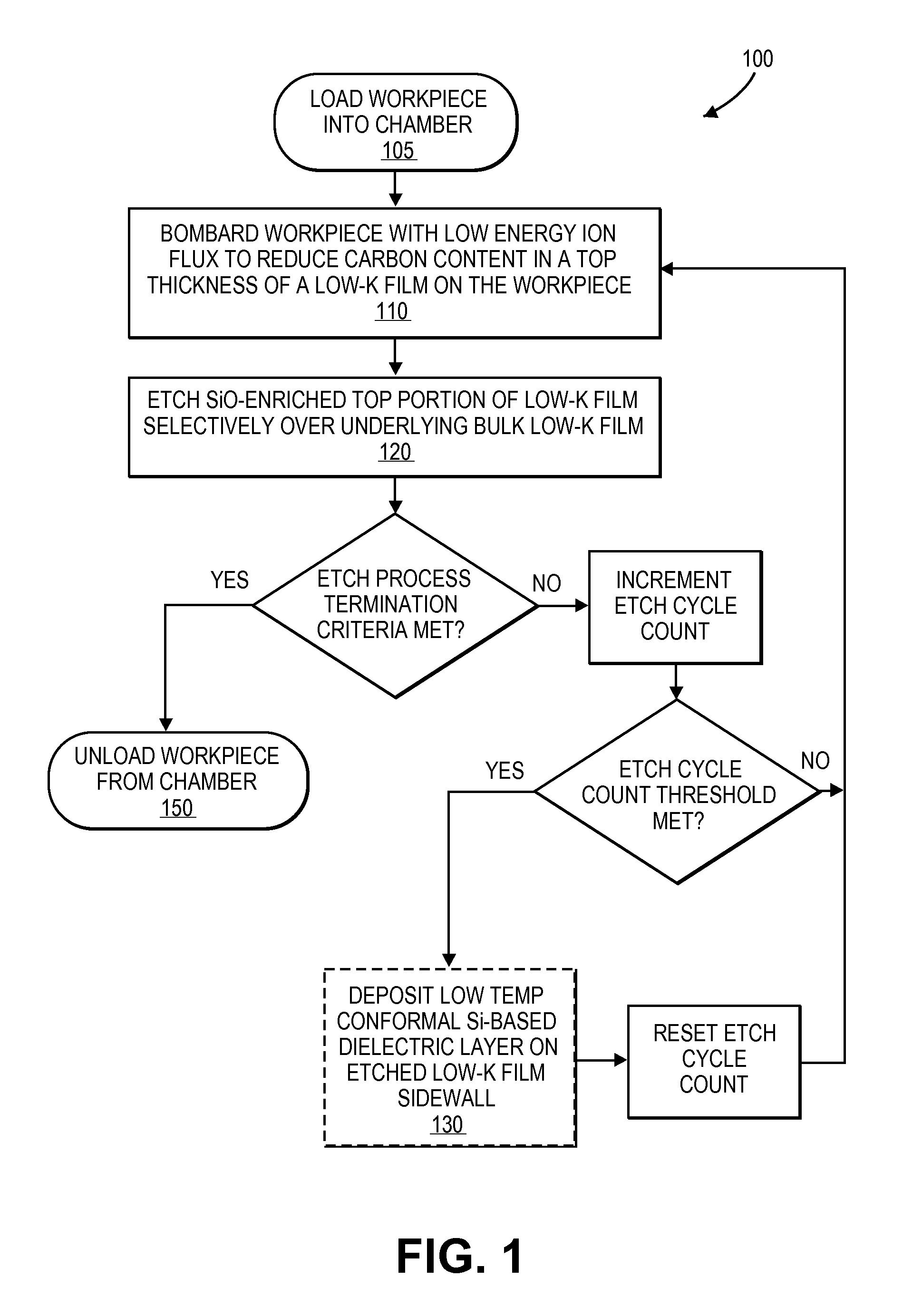
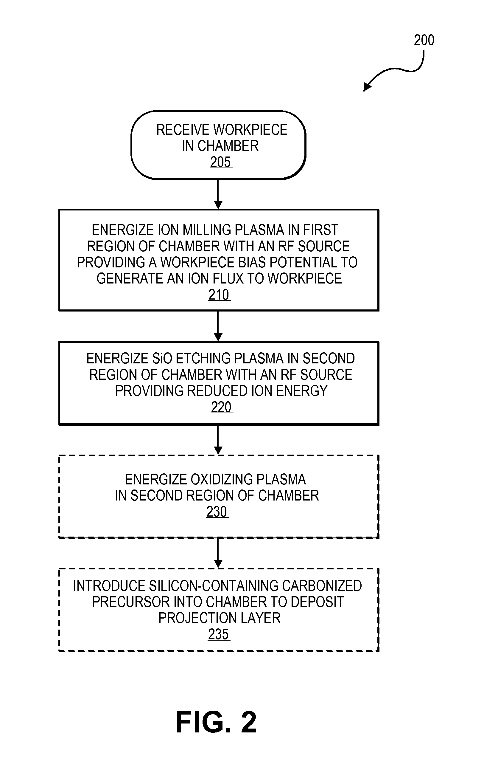
[0023]Generally, embodiments of the plasma etch methods described herein leverage damage mechanisms to etch low-k (and other dielectric) materials and leave a remainder of the etched film in good condition. Embodiments of the plasma etch methods described herein cyclically perform at least two separate plasma-based operations in-vaccuo (i.e., without breaking vacuum), and preferably in a same chamber for greatest throughput advantage. During one of these operations, an anisotropic (directional) plasma modifies the bulk structure and / or composition of a portion of the dielectric film being etched to be more like silicon dioxide (SiO2), or a silicon sub-oxide (SiOx). This film modification operation may be conceptualized as controllably and selectively damaging a portion of the dielectric film with the first plasma conditions. During a second of these operations, an isotropic (non-directional) condition removes the modified film portion (having the modified structure or composition) s...
PUM
| Property | Measurement | Unit |
|---|---|---|
| Temperature | aaaaa | aaaaa |
| Temperature | aaaaa | aaaaa |
| Bias potential | aaaaa | aaaaa |
Abstract
Description
Claims
Application Information