Organic light-emitting diode display device

a light-emitting diode and display device technology, applied in the direction of solid-state devices, semiconductor devices, thermoelectric devices, etc., can solve the problems of low process efficiency of oled display devices with the four color organic emission layers, short life span, and low luminous efficiency of sky blue organic materials, so as to improve process efficiency, increase life span and luminous efficiency, and wide color reproduction range

Active Publication Date: 2013-05-02
LG DISPLAY CO LTD
View PDF26 Cites 52 Cited by
  • Summary
  • Abstract
  • Description
  • Claims
  • Application Information

AI Technical Summary

Benefits of technology

[0024]An object of the present disclosure is to provide an OLED display device capable of ensuring a wide color reproduction range while significantly increasin

Problems solved by technology

If a blue emission material layer is made of a deep blue organic material, the deep blue organic material has an excellent color reproduction range, but has a shorter life span and lower luminous efficiency than a sky blue organic material.
Meanwhile, the OLED display device 10 with the f

Method used


Image

  • Organic light-emitting diode display device
  • Organic light-emitting diode display device
  • Organic light-emitting diode display device

Examples


first embodiment

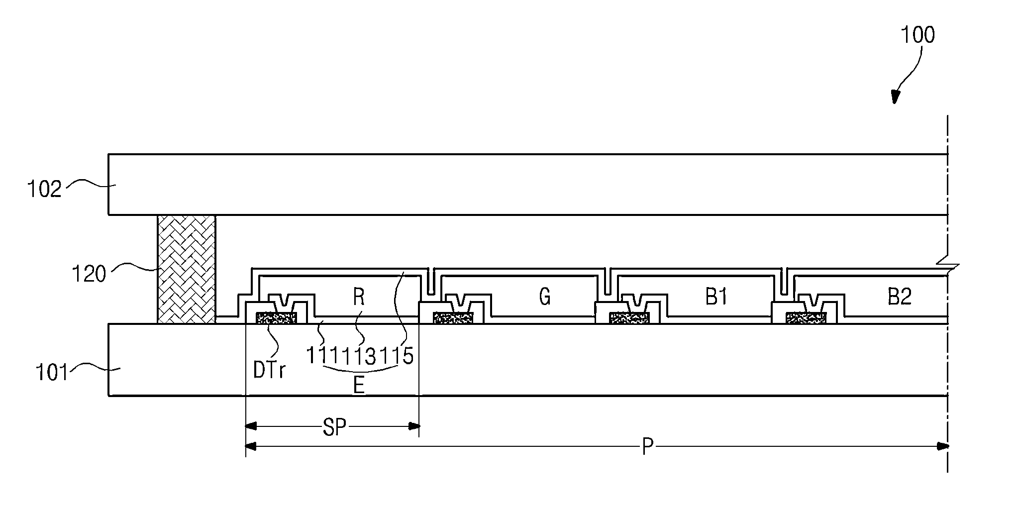
[0089]FIG. 4 is a view schematically illustrating the cross-sections of OLED display devices of red (R), green (G), deep blue (B1), and sky blue (B2) sub-pixels R-SP, G-SP, B1-SP, and B2-SP, according to a first embodiment of the present invention.

[0090]As shown in FIG. 4, each of the R, G, B1, and B2 sub-pixels R-SP, G-SP, B1-SP, and B2-SP has a stacked structure including a first electrode 111, a hole injection layer (HIL), a hole transport layer (HTL), a R, G, B1, or B2 emission material layer 200a, 200b, or 200c, an electron transport layer (ETL), an electron injection layer (EIL), and a second electrode 115.

[0091]The first electrode 111 has a double layer structure of a reflection layer 111a and a transparent layer 111b. The reflection layer 111a may be formed of a metal, such as aluminum (Al), a tantalum (Ta), silver (Ag), etc.

[0092]The transparent layer 111b may be preferably formed of a transparent, conductive material, for example, indium tin oxide (ITO) or indium zinc oxid...

second embodiment

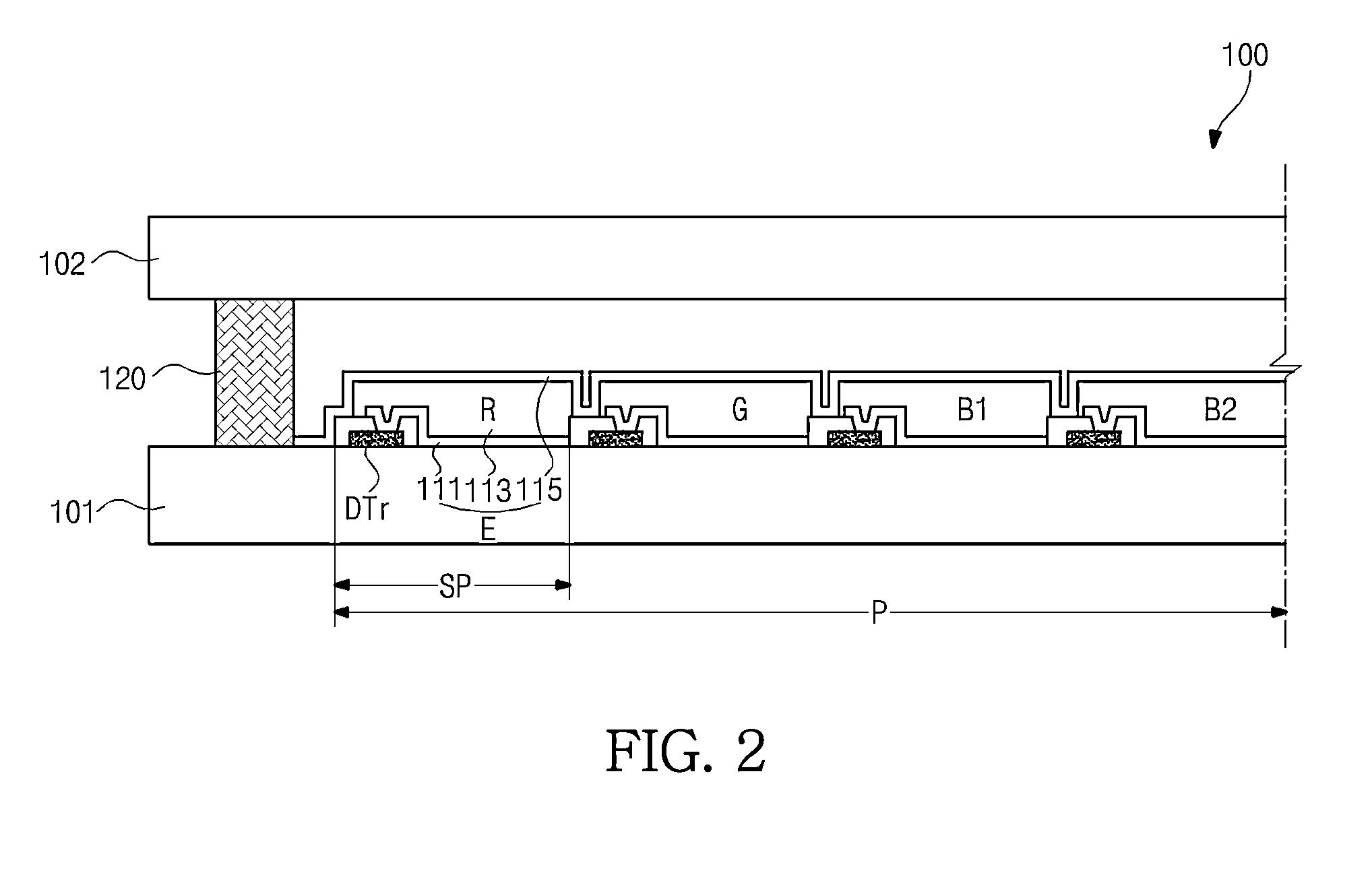
[0109]FIG. 6 is a view schematically illustrating the cross-sections of OLED display devices of red (R), green (G), deep blue (B1), and sky blue (B2) sub-pixels, according to a second embodiment of the present invention.

[0110]As shown in FIG. 6, each of the R, G, B1, and B2 sub-pixels R-SP, G-SP, B1-SP, and B2-SP has a stacked structure including a first electrode 111, a hole injection layer (HIL), a hole transport layer (HTL), a R, G, B1, or B2 emission material layer 200a, 200b, or 300, an electron transport layer (ETL), an electron injection layer (EIL), and a second electrode 115.

[0111]The first electrode 111 has a double layer structure of a reflection layer 111a and a transparent layer 111b. The reflection layer 111a may be formed of a metal, such as aluminum (Al), a tantalum (Ta), silver (Ag), etc.

[0112]The transparent layer 111b may be preferably formed of a transparent, conductive material, for example, indium tin oxide (ITO) or indium zinc oxide (IZO), having a relatively ...


PUM


Abstract

Provided is an organic light-emitting diode (OLED) display device having sub-pixels with four colors. When a B1 sub-pixel that represents deep blue and a B2 sub-pixel that represents sky blue are formed, by using a high efficiency blue organic material to form the same emission material layers in both the B1 and B2 sub-pixels such that a microcavity effect is implemented only in the B2 sub-pixel and a sky blue peak is extracted from the high efficiency blue organic material of the B2 sub-pixel, the emission material layer of the B2 sub-pixel represents sky blue. Therefore, a process of depositing emission material layers is simplified, which leads to a short process time and a reduction of the cost of materials, resulting in improvement in process efficiency of the OLED display device.

Description

[0001]The present application claims the priority benefit of Korean Patent Application No. 10-2011-0112725 filed in the Republic of Korea on Nov. 1, 2011, which is hereby incorporated by reference in their entirety.BACKGROUND[0002]1. Field of the Disclosure[0003]The present disclosure relates to an organic light-emitting diode (OLED) display device, and more particularly, to an organic light-emitting diode (OLED) display device having sub-pixels with four colors.[0004]2. Discussion of the Related Art[0005]A cathode ray tube (CRT) has been widely used as a display device for a long time. However, lately, flat panel displays, such as a plasma display panel (PDP), a liquid crystal display (LCD), and an organic light-emitting diode (OLED) display device, have been developed as a display device with which can replace the CRT, and are widely used.[0006]Among flat panel displays, the OLED display device which is a self-luminous device, can be manufactured as a light-weighted and slim produ...

Claims


Application Information

Patent Timeline
IPC IPC(8): H01L51/50H01L33/08
CPCH01L27/3213H01L51/5265H10K59/351H10K50/852H10K50/805H10K50/11H10K50/30
Inventor KIM, YONG-CHULYOO, JUHN-SUK
Owner LG DISPLAY CO LTD
Why Eureka
Try Eureka