Sige HBT and method of manufacturing the same

a technology of hbt and base region, applied in the field of hbt manufacturing, can solve the problems of low noise and low cost rf, the increase of the resistance of the base region, and the inability of conventional si-based devices to meet the new requirements of performance specifications, etc., and achieves the effect of increasing the thickness of the extrinsic base region, reducing the resistance of the base region, and high cut-off frequency

Active Publication Date: 2013-05-09
SHANGHAI HUAHONG GRACE SEMICON MFG CORP
View PDF2 Cites 2 Cited by
  • Summary
  • Abstract
  • Description
  • Claims
  • Application Information

AI Technical Summary

Benefits of technology

[0010]The method of manufacturing SiGe HBT of the present invention is compatible with CMOS processes. The thickness of the extrinsic base region is increased and hence the base region resistance is reduced by forming polysilicon gates having a thickness of greater than 150 nm using the process for forming polysilicon gates in a MOSFET, while a thin SiGe epitaxial layer is maintained to keep a high cut-off frequency. Further, instead of using an even N-type buried layer typically formed in a conventional device, the SiGe HBT of the present invention only forms buried layers (referred to as pseudo buried layers) under the field oxides on both sides of the active area, and then heavily dopes the pseudo buried layers with N-type impurities, and forms deep contact holes directly connecting to the pseudo buried layers in the field oxides to pick up the collector region, so there is no need to use the active area to pick up the electrode of the buried layer, and the size and area of the device is extremely reduced. The SiGe HBT and its manufacturing method of the present invention can reduce the base region resistance of the SiGe HBT so as to reduce the power consumption and increase the maximum oscillation frequency of the device without affecting its cut-off frequency.

Problems solved by technology

As demands for good performance, low noise and low cost RF components in modem communications increase, conventional Si-based devices can no longer meet the new requirements of performance specifications, output power and linearity, and thus have been replaced by power SiGe HBTs (Silicon-Germanium Heterojunction Bipolar Transistors) which are playing an important role in power amplifiers having a wider band and higher frequency.
Therefore, it has been a most important technical problem to reduce the base region resistance of a SiGe HBT so as to reduce the power consumption and increase the maximum oscillation frequency of the device.
A thin base region will lead to an increase in the base region resistance, which is against the improvement of other performances of the device.

Method used


Image

  • Sige HBT and method of manufacturing the same
  • Sige HBT and method of manufacturing the same
  • Sige HBT and method of manufacturing the same

Examples


Embodiment Construction

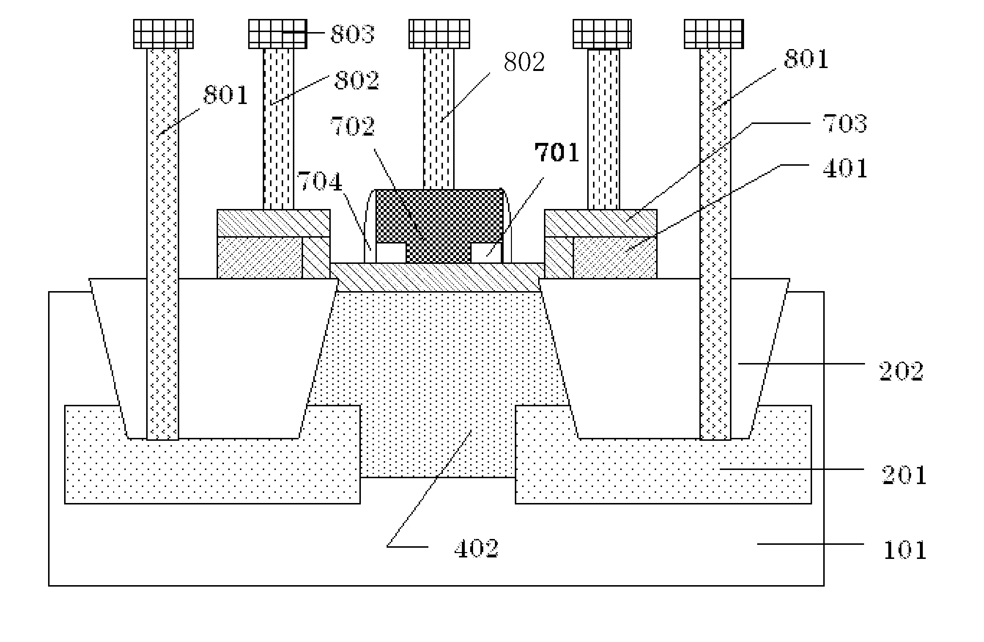
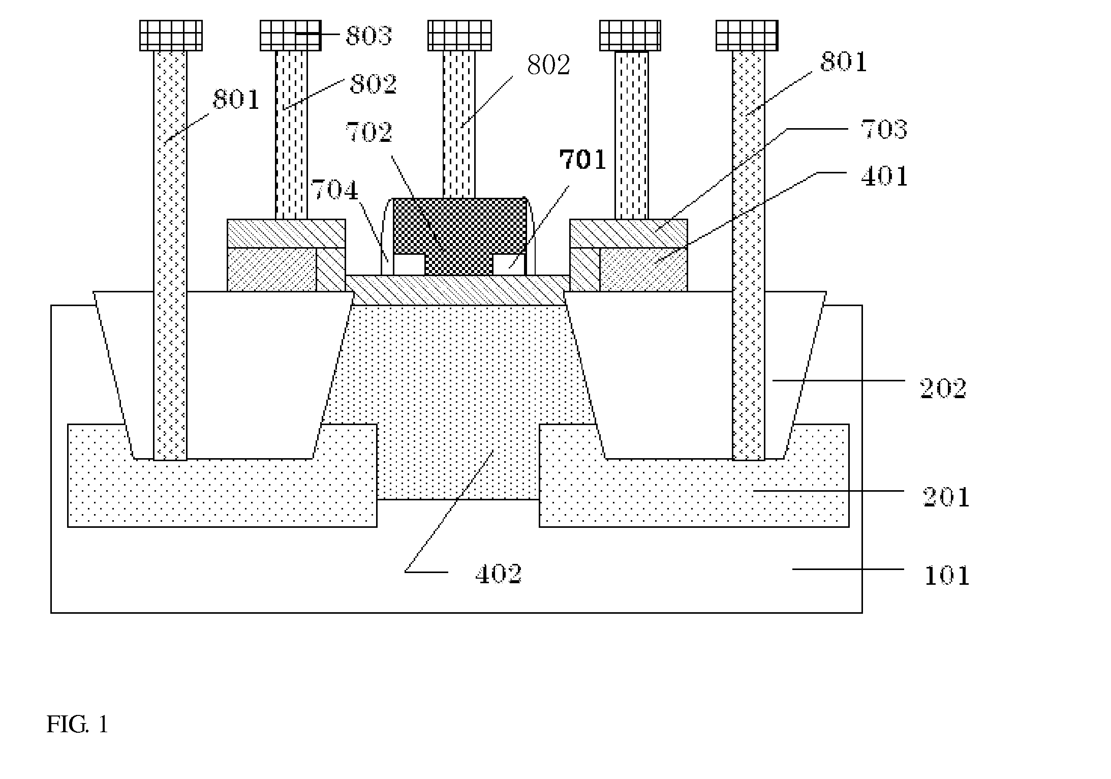
[0015]FIG. 1 is a schematic diagram of the SiGe HBT of the present invention. As shown in FIG. 1, a collector region 402 and pseudo buried layers 201 are formed in a silicon substrate 101. A shallow trench field oxide 202 is formed above each pseudo buried layer 201. A polysilicon gate 401 is formed above each shallow trench field oxide 202. A base region 703 is formed on the polysilicon gates 401 and the collector region 402. Emitter region isolation oxides 701 are formed on the base region 703 and are located above the collector region 402. An emitter region 702 is formed on the emitter region isolation oxides 701 and a part of the base region 703 between the emitter region isolation oxides 701. Spacers 704 are formed on sidewalls of the emitter region 702 and emitter region isolation oxides 701. The collector region 402 is adjacent to the shallow trench field oxides 202 and the pseudo buried layers 201. Each pseudo buried layer 201 is picked up by a deep contact hole 801 and is c...


PUM


Abstract

A SiGe HBT is disclosed, which includes: a silicon substrate; shallow trench field oxides formed in the silicon substrate; a pseudo buried layer formed at bottom of each shallow trench field oxide; a collector region formed beneath the surface of the silicon substrate, the collector region being sandwiched between the shallow trench field oxides and between the pseudo buried layers; a polysilicon gate formed above each shallow trench field oxide having a thickness of greater than 150 nm; a base region on the polysilicon gates and the collector region; emitter region isolation oxides on the base region; and an emitter region on the emitter region isolation oxides and a part of the base region. The polysilicon gate is formed by gate polysilicon process of a MOSFET in a CMOS process. A method of manufacturing the SiGe HBT is also disclosed.

Description

CROSS-REFERENCE TO RELATED APPLICATIONS[0001]This application claims the priority of Chinese patent application number 201110342684.X, filed on Nov. 3, 2011, the entire contents of which are incorporated herein by reference.TECHNICAL FIELD[0002]The present invention relates to the field of semiconductor manufacturing, and more particularly, to a SiGe HBT and its manufacturing method.BACKGROUND ART[0003]As demands for good performance, low noise and low cost RF components in modem communications increase, conventional Si-based devices can no longer meet the new requirements of performance specifications, output power and linearity, and thus have been replaced by power SiGe HBTs (Silicon-Germanium Heterojunction Bipolar Transistors) which are playing an important role in power amplifiers having a wider band and higher frequency.[0004]Although the frequency performance of SiGe HBTs is not as good as GaAs-based devices, SiGe HBTs have well solved the heat dissipation problem of power am...

Claims


Application Information

Patent Timeline
Patent Type & Authority Applications(United States)
IPC IPC(8): H01L29/737H01L21/331
CPCH01L29/66242H01L29/0821H01L29/7371
Inventor LIU, DONGHUADUAN, WENTINGQIAN, WENSHENGHU, JUNSHI, JING
Owner SHANGHAI HUAHONG GRACE SEMICON MFG CORP
Why Eureka
Try Eureka