
Electrically conductive material and electronic device using same

a technology of electrical conductive materials and electronic devices, applied in the direction of metal/alloy conductors, electrical apparatus construction details, conductors, etc., to achieve the effect of effective us

Inactive Publication Date: 2013-05-09
DENSO CORP
View PDF0 Cites 16 Cited by
  • Summary
  • Abstract
  • Description
  • Claims
  • Application Information

AI Technical Summary

Benefits of technology

This patent aims to prevent short circuits in semiconductor devices that are produced by laminating resin layers and heating them under pressure. The invention proposes the use of heat-releasing filled vias in the circuit board that can effectively dissipate the heat generated by the semiconductor chip. By controlling the size of the heat-releasing filled vias and the heat-receiving surface, the short circuit problem can be effectively prevented. Additionally, the invention also provides an electrically conductive material that can be used in the production of semiconductor devices which include heat-releasing filled vias in a multilayer circuit board.

Problems solved by technology

However, the metal powder are not completely consumed during this alloy production step, and thus some of the unused Sn component may remain in the conductive material.

Method used


Image

  • Electrically conductive material and electronic device using same
  • Electrically conductive material and electronic device using same
  • Electrically conductive material and electronic device using same

Examples


examples

[0102]The present invention will be further described with reference to the examples thereof.

example 11

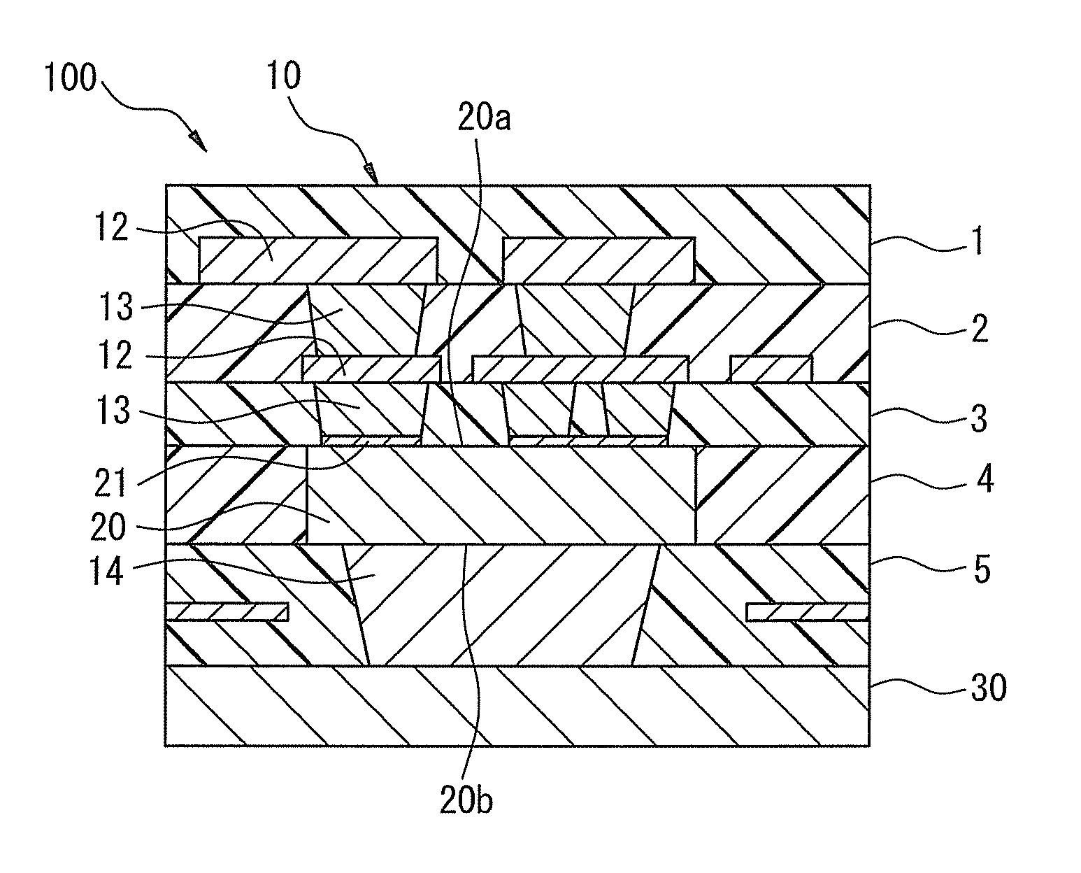
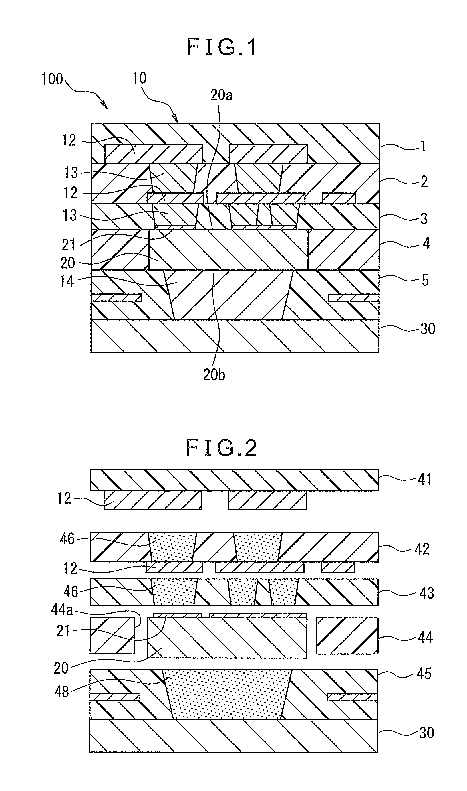
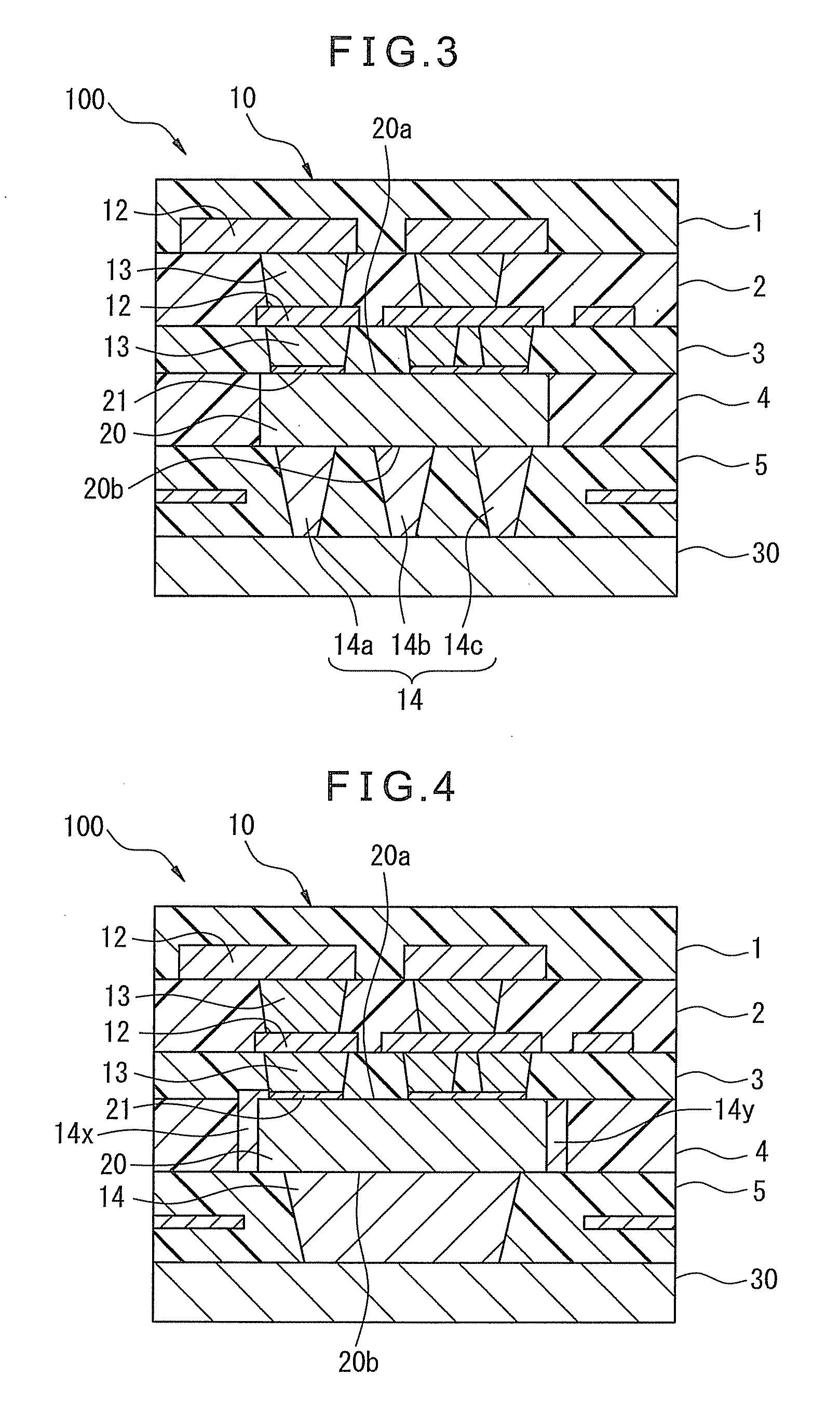
[0128]The procedure described in Examples 1 to 5 described above was repeated in this example. However, in this example, a metal paste having an atomicity ratio (%) of Sn to Cu and Sn of 30% was prepared to produce the semiconductor device 100 shown in FIG. 1. The tests showed that the operating characteristics of the semiconductor chip 20 were normal and acceptable.

[0129]In this example, when the metal paste used was sintered, the XRD analysis showed that the sintered product was substantially formed from Cu3Sn alloy. Further, the electron microscopic inspection and the XRD analysis showed that a Sn diffusion layer (Cu3Sn) was formed on a surface of the heat radiation member 30 opposed to the heat-releasing via 14.

[0130]Further, as is appreciated from the state diagram (not shown) of the Cu—Sn binary alloy, when Cu and Sn are reacted in the Cu—Sn binary alloy, if an atomicity ratio (%) of Sn to Cu and Sn is in the range of 20 to 45%, Cu3Sn is substantially formed stably. In this co...


PUM

PropertyMeasurementUnit
temperatureaaaaaaaaaa

Abstract

An electrically conductive material used in the formation of heat-releasing filled via holes in an electronic component-incorporated multilayer circuit board with a heat radiation member, in which the electrically conductive material comprises metal particles as a conductive metal which is a mixture of a first conductive metal consisting of silver (Ag) or copper (Cu) and a second conductive metal consisting of tin (Sn), and a ratio of the atomicity of tin to the atomicity of silver or copper and tin is 27 to 40%, and an electronic device using the same.

Description

CROSS-REFERENCE TO RELATED APPLICATION[0001]This application is based on Japanese Patent Application No. 2011-243231 filed on Nov. 7, 2011, and Japanese Patent Application No. 2012-167062 filed on Jul. 27, 2012, the disclosures of which are incorporated herein by reference in their entirety.BACKGROUND OF THE INVENTION[0002]1. Field of the Invention[0003]The present invention relates to an electrically conductive material used in the formation of heat-releasing filled via holes in an electronic component-incorporated multilayer circuit board with a heat radiation member, and an electronic device, typically a semiconductor device, comprising an electronic component-incorporated multilayer circuit board with heat-releasing filled via holes, formed from the electrically conductive material, and a heat radiation member.[0004]2. Description of the Related Art[0005]Hitherto, a wide variety of semiconductor devices which comprise a multilayer circuit board having incorporated therein a semi...

Claims


Application Information

Patent Timeline
Patent Type & Authority Applications(United States)
IPC IPC(8): H01B1/02H05K7/20
CPCH01B1/02H01B1/026H05K3/4069H05K1/0206H05K1/186H05K7/20409H01L2224/18
Inventor TADA, KAZUOKONDOH, KOUJIFUJIHARA, KOUHEISHIRAISHI, YOSHIHIKO
Owner DENSO CORP
Learn More