Method of cleaning multilayer copper wirings in ultra large scale integrated circuits after chemical-mechanical polishing

a multi-layer, integrated circuit technology, applied in the direction of cleaning process and apparatus, cleaning liquids, chemistry apparatus and processes, etc., can solve the problems of unfavorable environmental protection, unfavorable environmental protection, and loss of dielectric materials in copper interconnections, etc., to achieve easy operation and pollution-free

Inactive Publication Date: 2013-05-16
HEBEI UNIV OF TECH
View PDF4 Cites 1 Cited by
  • Summary
  • Abstract
  • Description
  • Claims
  • Application Information

AI Technical Summary

Benefits of technology

[0010]In view of the above-described problems, it is one objective of the invention to provide a method of cleaning multilayer copper wirings in ULSI after CMP, which has an easy operation, pollution free, and cleanness.

Problems solved by technology

Dirt such as grains, organic matters, and metal ions after CMP may cause fatal damages on integrated components.
Conventional commercial cleaning solutions or HF cleaning solutions used to remove dirt easily causes loss of dielectric materials and unnecessary inductive disturbance in copper interconnections.
Furthermore, uneven oxidation caused by polishing solution residues is one of the urgent problems to be solved.
Newly exposed surface of multilayer copper wirings after CMP has high surface energy, and tends to adsorb a layer of matters to achieve a steady state, during which surrounding grains are first physically adsorbed on the surface via van der Waals force which is so weak that grains are easily removable; as the distance becoming closer, energy is quickly released and chemical adsorptions are formed until grains are finally combined together with copper surface, thereby being difficult to be removed by conventional cleaning methods.
However, polishing solution residues after CMP and adsorbed grains seriously affect the cleanness of copper surface, parts of surface continue reacting with surrounding grains to form corrosion circles.
Furthermore, defect points on copper surface have high energy and corrosion rate, and are easy to form corrosion pits, at the same time, copper surface exposed in the air are quickly oxidized, thereby resulting in high resistance, heat release, and electromigration, and finally lowering the reliability of electric elements.

Method used


Image

  • Method of cleaning multilayer copper wirings in ultra large scale integrated circuits after chemical-mechanical polishing

Examples


example 1

[0045]Prepare a cleaning solution, the cleaning solution comprising 0.1 wt. % of a nonionic surfactant, 7 wt. % of a corrosion inhibitor, 0.4 wt. % of a chelating agent, and deionized water.

example 2

[0046]Prepare a cleaning solution, the cleaning solution comprising 5 wt. % of a nonionic surfactant, 0.1 wt. % of a corrosion inhibitor, 0.6 wt. % of a chelating agent, and deionized water.

example 3

[0047]Prepare a cleaning solution, the cleaning solution comprising 3 wt. % of a nonionic surfactant, 5 wt. % of a corrosion inhibitor, 0.1 wt. % of a chelating agent, and deionized water.

[0048]Cleaning effects of the cleaning solution prepared in above examples using the method of cleaning multilayer copper wirings in ultra large scale integrated circuits after chemical-mechanical polishing are concluded hereinbelow:

[0049]1. copper wirings of wafers had no oxidation on the surface;

[0050]2. Observations under a microscope at a magnification of 100× showed that copper wirings of wafers had no uneven corrosion, corrosion circles, or pits.

[0051]3. Cu2+, Fe3+, Ni2+ and other metal ions on the surfaces of the copper wirings of wafers formed very stable chelats and complexes, the determination by graphite furnace atomic adsorption spectrometry showed that contents of Cu2+, Fe3+, Ni2+ and other metal ions on the surfaces have been reduced to a ppb level below.

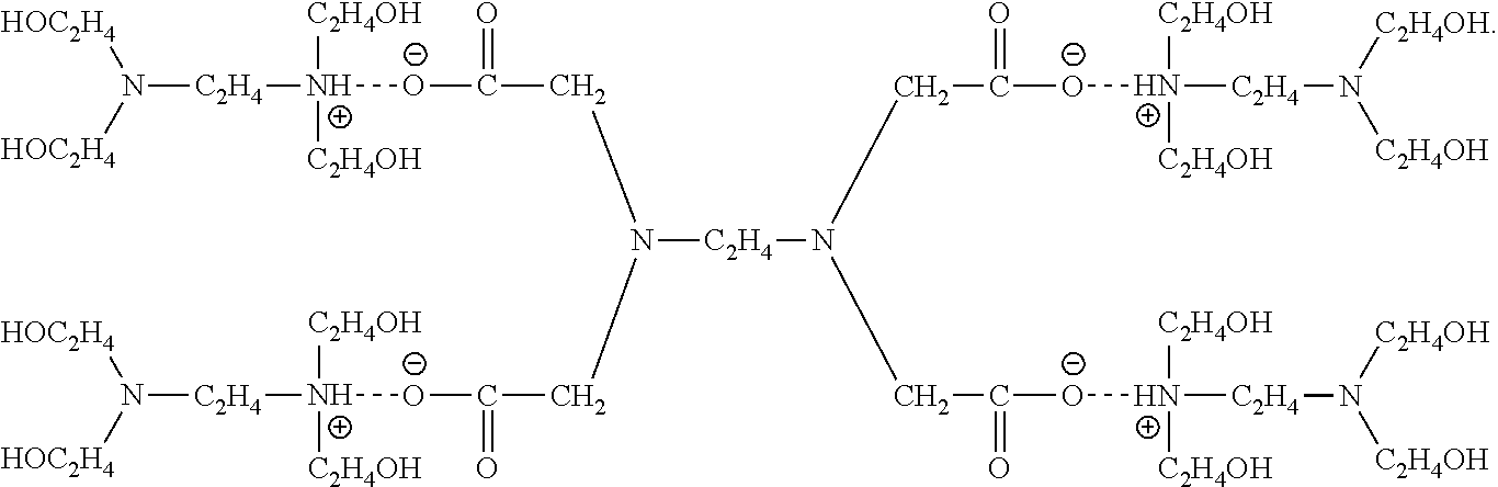
[0052]Working principles: the ...


PUM


Abstract

A method of cleaning multilayer copper wirings in ultra large scale integrated circuits after chemical-mechanical polishing, the method including: a) preparing a cleaning solution, the cleaning solution including between 0.1 and 5 wt. % of a nonionic surfactant, between 0.1 and 7 wt. % of a corrosion inhibitor, and between 0.1 and 0.6 wt. % of a chelating agent in deionized water; b) adjusting the pH value of the cleaning solution to between 7 and 8 using triethanolamine; c) during the production of ULSI, after the chemical-mechanical polishing step, washing the multilayer copper wirings with the cleaning solution at a flow rate of between 500 and 5000 mL/min for between 0.5 and 1 min; d) ultrasonic washing in the presence of deionized water under following conditions: 60 Hz frequency of ultrasound, 50° C. temperature, and between 0.5 and 1 min ultrasonic time; and e) drying the multilayer copper wirings.

Description

CROSS-REFERENCE TO RELATED APPLICATIONS[0001]This application is a continuation-in-part of International Patent Application No. PCT / CN2010 / 080473 with an international filing date of Dec. 30, 2010, designating the United States, now pending, and further claims priority benefits to Chinese Patent Application No. 201010232256.7 filed Jul. 21, 2010. The contents of all of the aforementioned applications, including any intervening amendments thereto, are incorporated herein by reference. Inquiries from the public to applicants or assignees concerning this document or the related applications should be directed to: Matthias Scholl P.C., Attn.: Dr. Matthias Scholl Esq., 14781 Memorial Drive, Suite 1319, Houston, Tex. 77079.BACKGROUND OF THE INVENTION[0002]1. Field of the Invention[0003]The invention relates to a cleaning method, and more particularly to a method of cleaning multilayer copper wirings in ultra large scale integrated circuits (ULSI) after chemical-mechanical polishing (CMP)....

Claims


Application Information

Patent Timeline
Patent Type & Authority Applications(United States)
IPC IPC(8): B08B3/12
CPCH01L21/02074B08B3/12H01L21/7684
Inventor LIU, YULINGHUANG, YANYANTAN, BAIMEIGAO, BAOHONGZHOU, QIANG
Owner HEBEI UNIV OF TECH
Why Eureka
Try Eureka