However, wires (interconnects) that connect together transistors degrade in performance with “scaling”.
The situation today may be that wires dominate performance, functionality and
power consumption of ICs.
However, there are many barriers to practical implementation of 3D stacked chips.
Copper or Aluminum wiring levels, in fact, can get damaged when exposed to temperatures higher than ˜400° C. If one would like to arrange transistors in 3 dimensions along with wires, it has the challenge described below.
When the Top
Transistor Layer may be constructed using Temperatures higher than 700° C., it can damage the Bottom Wiring Layer.Due to the above mentioned problem with forming
transistor layers above wiring
layers at temperatures lower than 400° C., the
semiconductor industry has largely explored alternative architectures for 3D stacking.
Unfortunately, the size of Contacts to the other Layer may be large and the number of these Contacts may be small.
This low
connectivity between
layers may be because of two reasons: (i) Landing pad size needs to be relatively large due to alignment issues during
wafer bonding.
Etching deep holes in
silicon with small lateral dimensions and filling them with
metal to form TSVs may be not easy.
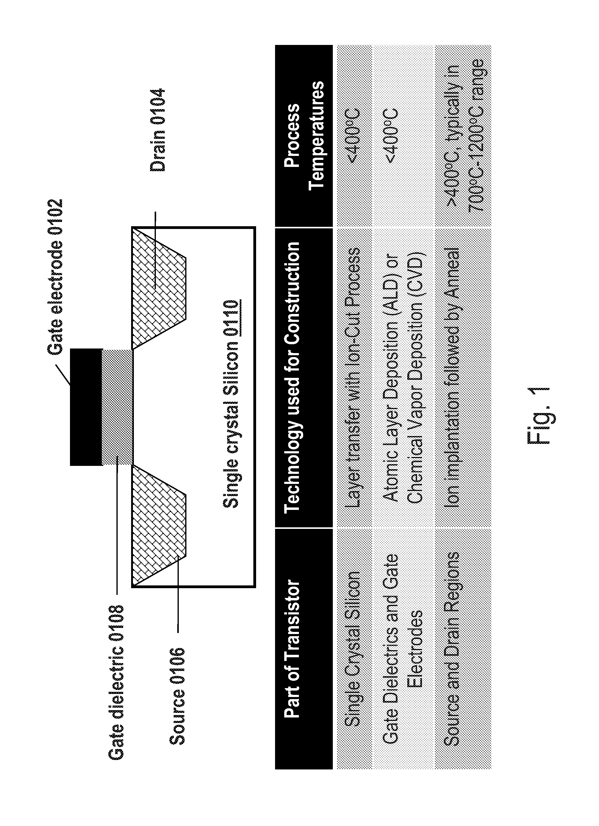
Unfortunately, however, almost all
semiconductor devices in the market today (logic,
DRAM,
flash memory) utilize horizontal (or planar) transistors due to their many advantages, and it may be difficult to convince the industry to move to vertical
transistor technology.
A process flow may be utilized to transfer this top transistor layer atop the bottom wiring and transistor layers at temperatures less than 400° C. Unfortunately, since transistors are fully formed prior to bonding, this scheme suffers from misalignment issues.
While Topol describes techniques to reduce misalignment errors in the above paper, the techniques of Topol still suffer from misalignment errors that limit contact dimensions between two chips in the stack to >130 nm.
Unfortunately, however, these technologies have higher defect density compared to standard
single crystal silicon.
This higher defect density degrades transistor performance.
However, the approach described by Hubert has some challenges including the use of difficult-to-manufacture
nanowire transistors, higher defect densities due to formation of Si and SiGe layers atop each other, high temperature
processing for long times, and difficult manufacturing.
None of these products are true 3DICs.
In particular, yield and reliability of extremely complex three dimensional systems will have to be addressed, particularly given the yield and reliability difficulties encountered in complex
Application Specific Integrated Circuits (ASIC) built in recent deep submicron process generations.
However, wires (interconnects) that connect together transistors degrade in performance with “scaling”.
The situation today may be that wires dominate performance, functionality and
power consumption of ICs.
Irrespective of the technique used to construct 3D stacked integrated circuits or chips, heat removal may be a serious issue for this technology.
Removing the heat produced due to this
power density may be a significant challenge.
In addition, many heat producing regions in 3D stacked integrated circuits or chips have a high
thermal resistance to the
heat sink, and this makes heat removal even more difficult.

