Supercharge Your Innovation With Domain-Expert AI Agents!

Organic light-emitting diode including multi-layered hole transporting layer, and flat display device including the organic light-emitting diode

a light-emitting diode and multi-layer technology, applied in the direction of solid-state devices, thermoelectric devices, organic chemistry, etc., can solve the problems of reduced thermal stability of organic materials, low efficiency of formed devices, and reduced lifetime of organic light-emitting diodes, etc., to achieve long lifetime and high luminous efficiency

Active Publication Date: 2013-06-20
SAMSUNG DISPLAY CO LTD
View PDF2 Cites 29 Cited by
  • Summary
  • Abstract
  • Description
  • Claims
  • Application Information

AI Technical Summary

Benefits of technology

This patent text describes an organic light-emitting diode (OLED) that has very high luminous efficiency and can stay bright for a long time. It includes a special layered structure called a hole transport layer that helps to balance the injection and flow of holes and electrons. This results in a more effective and efficient OLED.

Problems solved by technology

However, charges are excessively injected, and thus a formed device may have low efficiency and a short lifetime.
However, in a phosphorescent organic light-emitting diode having a PIN structure, the thermal stability of an organic material is relatively reduced, and thus the organic light-emitting diode has a reduced lifetime.
Also, because (unlike a typical inorganic semiconductor) the phosphorescent organic light-emitting diode having the PIN structure does not have crystallinity, it is difficult to reproduce current control.
However, owing to the inclusion of the HIL doped with the p-type dopant and thus injection of excess holes, the organic EL device has reduced lifetime and efficiency.
However, in an organic EL device having a first hole transport layer / p-doped first hole transport layer / p-doped second hole transport layer / second hole transport layer structure, it is difficult to control the balance of charges formed in the EML.

Method used


Image

  • Organic light-emitting diode including multi-layered hole transporting layer, and flat display device including the organic light-emitting diode
  • Organic light-emitting diode including multi-layered hole transporting layer, and flat display device including the organic light-emitting diode
  • Organic light-emitting diode including multi-layered hole transporting layer, and flat display device including the organic light-emitting diode

Examples


example 1

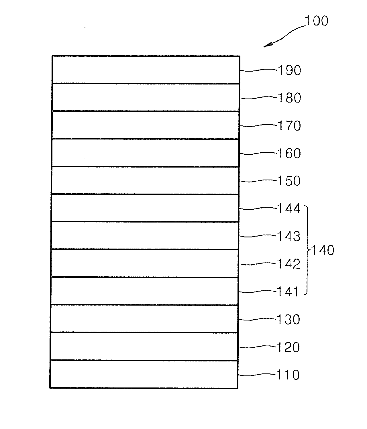
[0147]A 15 Ω / cm2 (1200 Å) ITO glass substrate (manufactured by Corning) as an anode was cut into a size of 50 mm×50 mm×0.7 mm, ultrasonically cleansed using isopropyl alcohol and pure water for 5 minutes each, irradiated with a UV ray for 30 minutes, cleansed by being exposed to ozone, and the ITO glass substrate was placed on a vacuum deposition device.

[0148]A first charge generation layer with a thickness of about 100 Å was formed by vacuum co-depositing Compound 301 and Compound 501 in a ratio of 98:2 by weight on the ITO glass substrate. A first layer with a thickness of about 400 Å was formed by vacuum depositing Compound 35 on the first charge generation layer. A second charge generation layer with a thickness of about 200 Å was formed by vacuum co-depositing Compound 301 and Compound 501 in a ratio of 98:2 by weight on the first layer. A second layer with a thickness of about 400 Å was formed by vacuum depositing Compound 35 on the second charge generation layer.

[0149]A buffe...

example 2

[0152]An OLED was manufactured in the same manner as in Example 1, except that Compound 2 was used for vacuum deposition instead of Compound 35 during formation of each of the first layer and the second layer.

example 3

[0153]An OLED was manufactured in the same manner as in Example 1, except that Compound 14 was used for vacuum deposition instead of Compound 35 during formation of the second layer.


PUM


Abstract

An organic light-emitting diode includes a first electrode; a second electrode facing the first electrode; an emission layer (EML) between the first electrode and the second electrode; a first charge generation layer between the EML and the first electrode and including a first compound and a first charge generation material; a first layer between the EML and the first charge generation layer and including a second compound; a second charge generation layer between the EML and the first layer and including a third compound and a second charge generation material; a second layer between the EML and the second charge generation layer and including a fourth compound; and a buffer layer between the EML and the second layer. The first and third compounds each independently includes a compound represented by Formula 1, and the second and fourth compounds each independently includes a compound represented by Formula 2.

Description

CROSS-REFERENCE TO RELATED PATENT APPLICATION[0001]This application claims priority to and the benefit of Korean Patent Application No. 10-2011-0137416, filed on Dec. 19, 2011 in the Korean Intellectual Property Office, the entire content of which is incorporated herein by reference.BACKGROUND[0002]1. Technical Field[0003]Embodiment of the present invention relates to an organic light-emitting diode (OLED) including a multi-layered hole transporting layer and a flat display device including the organic light-emitting diode. More particularly, embodiments of the present invention relate to an OLED including a hole transporting layer that includes a plurality of layers formed using a hole transporting material and a charge generation material which have different energy levels from each other, and to a flat display device including the OLED.[0004]2. Description of the Related Art[0005]Organic light emitting diodes (OLEDs) are self-emission devices that have wide viewing angles, high c...

Claims


Application Information

Patent Timeline
IPC IPC(8): H01L51/54
CPCH01L51/006H01L51/0061H01L51/5064H01L51/0072H01L51/0067H10K85/636H10K85/633H10K85/654H10K85/6572H10K50/156C07D209/82
Inventor KHO, SAM-ILPARK, MIE-HWAKIM, HYOUNG-KUNKWAK, YOON-HYUNLIM, JA-HYUNCHU, CHANG-WOONGLEE, KWAN-HEE
Owner SAMSUNG DISPLAY CO LTD
Features
  • R&D
  • Intellectual Property
  • Life Sciences
  • Materials
  • Tech Scout
  • Unparalleled Data Quality
  • Higher Quality Content
  • 60% Fewer Hallucinations
Learn More