Semiconductor device, semiconductor device unit, active matrix substrate, liquid crystal panel, and liquid crystal display

a semiconductor device and active matrix technology, applied in static indicating devices, instruments, optics, etc., can solve the problem of low signal level when inactive, and achieve the effect of reducing layout space, reducing layout area, and reducing layout area

Active Publication Date: 2013-06-20
SHARP KK
View PDF3 Cites 10 Cited by
  • Summary
  • Abstract
  • Description
  • Claims
  • Application Information

AI Technical Summary

Benefits of technology

[0052]Advantageous Effects of Invention
[0053]As described above, a semiconductor device of the present invention is configured to include: a first electrode made of a material that is the same as a material of a channel layer of the transistor; a second electrode formed in an upper layer of the first electrode; a control signal line formed in an upper layer of the second electrode; a first insulating film provided between the first electrode and the second electrode; and a second insulating film provided between the second electrode and the control signal line, the second electrode being connected to a gate electrode of the transistor, the control signal line being supplied with a control signal from outside the semiconductor device, the bootstrap capacitor being formed in an o

Problems solved by technology

Meanwhile, these signals beco

Method used


Image

  • Semiconductor device, semiconductor device unit, active matrix substrate, liquid crystal panel, and liquid crystal display
  • Semiconductor device, semiconductor device unit, active matrix substrate, liquid crystal panel, and liquid crystal display
  • Semiconductor device, semiconductor device unit, active matrix substrate, liquid crystal panel, and liquid crystal display

Examples


embodiment 1

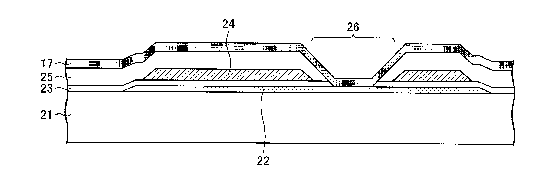
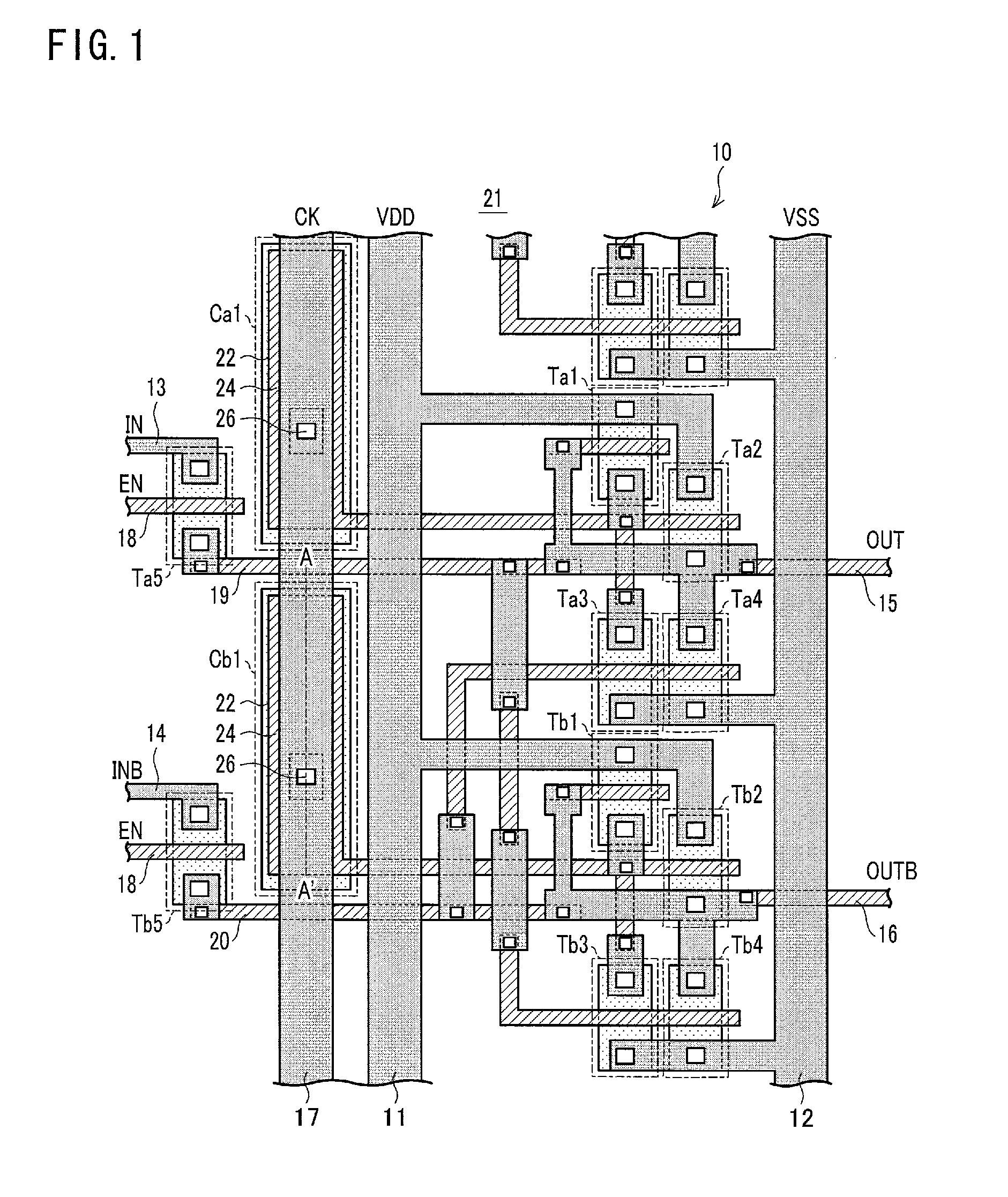
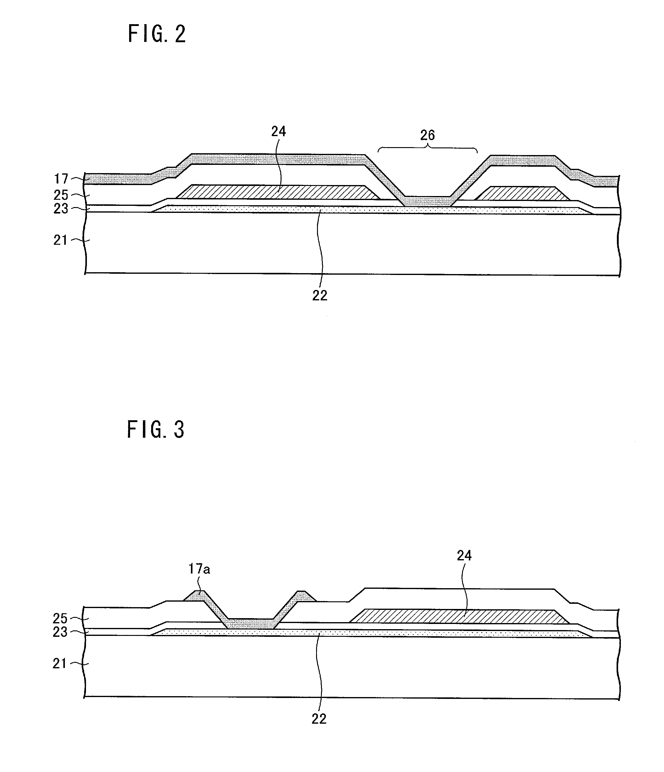
[0074]The following discusses one embodiment of the present invention, with reference to drawings. FIG. 1 is a plan view illustrating a layout pattern of the semiconductor device 10 in accordance with Embodiment 1 in a case where the semiconductor device 10 is viewed from above. The semiconductor device 10 includes a transistor Ta1, a transistor Ta2, a transistor Ta3, a transistor Ta4, a transistor Ta5, a transistor Tb1, a transistor Tb2, a transistor Tb3, a transistor Tb4, a transistor Tb5, a capacitor Ca1, and a capacitor Cb1. Specifically, the semiconductor device 10 is realized by formation of the above components on a substrate 21, as illustrated in FIG. 1.

[0075]Further, as illustrated in FIG. 1, on the substrate 21, the following lines are formed: a power supply line 11 for providing a power supply VDD, a power supply line 12 for providing a power supply VSS, an input line 13 for inputting an input signal IN, an input line 14 for inputting an inversion input signal INB, an out...

embodiment 2

[0119]The following discusses one embodiment of the present invention with reference to drawings. Embodiment 2 deals with a semiconductor device unit including a plurality of semiconductor devices 10 described above. Note that configurations other than configurations explained in Embodiment 2 are the same as those in Embodiment 1. Further, for convenience of explanation, members having identical functions as those illustrated in drawings of Embodiment 1 are given the same reference signs and explanations thereof are omitted.

[0120]FIG. 4 is a plan view illustrating a layout pattern of a semiconductor device unit 50 of Embodiment 2 in a case where the semiconductor device unit 50 is viewed from above. The semiconductor device unit 50 of Embodiment 2 includes a semiconductor device 10a and a semiconductor device 10b. The semiconductor device 10a and the semiconductor device 10b are aligned along a vertical direction.

[0121]The semiconductor device 10a includes a transistor Ta11, a trans...

embodiment 3

[0135]The following discusses one embodiment of the present invention with reference to drawings. Embodiment 3 deals with a liquid crystal display device including a liquid crystal panel to which a semiconductor device 10 or a semiconductor device unit of the above embodiments is mounted. Note that configurations other than configurations explained in Embodiment 3 are the same as those in Embodiments 1 and 2. Further, for convenience of explanation, members having identical functions as those illustrated in drawings of Embodiments 1 and 2 are given the same reference signs and explanations thereof are omitted.

[0136]FIG. 5 is a block diagram schematically illustrating one example configuration of a liquid crystal display device 100 of Embodiment 3. As illustrated in FIG. 5, the liquid crystal display device 100 includes a liquid crystal panel 101, and the display panel 101 includes a display section 102, a source driver 103 (driver circuit), a gate / CS driver 104 (driver circuit) and ...


PUM


Abstract

A semiconductor device (10) provided with at least a plurality of transistors and bootstrap capacitors (Ca1 and Cb1), the semiconductor device (10) includes: a semiconductor layer (22) made of the same material as a channel layer of each of the transistors; a capacitor electrode (24) formed in an upper layer of the semiconductor layer (22); and a clock signal line (17) formed in an upper layer of the capacitor electrode (24), the capacitor electrode (24) being connected to a gate electrode of each of the transistors, the clock signal line (17) being supplied with a clock signal (CK) from outside the semiconductor device (10), the capacitors (Ca1 and Cb1) each being formed in an overlap section where the semiconductor layer (22), the gate insulating film (23) and the capacitor electrode (24) overlap one another, the overlap section and the clock signal line (17) overlapping each other when viewed from above.

Description

TECHNICAL FIELD [0001]The present invention relates to a semiconductor device, a semiconductor device unit, an active matrix substrate, a liquid crystal panel, and a liquid crystal display device each of which includes a transistor and a bootstrap capacitor, and in particular, is related to a technique for reducing a layout area. Background Art[0002]Among liquid crystal display devices, some liquid crystal display devices include a liquid crystal panel where a display section and a peripheral circuit such as a driver circuit are fabricated on a single substrate. The liquid crystal display devices each including such a liquid crystal panel is capable of achieving simplification of a panel mounting process, reduction in mounting area which reduction leads to a narrower frame, a smaller size, and a smaller weight, and the like, as compared to conventional liquid crystal display devices for each of which an IC for realizing a peripheral circuit is provided externally but not on a glass ...

Claims


Application Information

Patent Timeline
IPC IPC(8): H01L49/02H01L27/04H01L33/08
CPCG02F1/13454G02F1/136277G09G3/3648G09G2310/0286H01L27/04H01L28/40G09G2310/08H01L27/1255G09G3/3611G09G3/3677G09G2310/0278G09G2310/0291H01L33/08
Inventor SASAKI, OSAMUMURAKAMI, YUHICHIROHSASAKI, YASUSHIYAMAMOTO, ETSUO
Owner SHARP KK
Why Eureka
Try Eureka