Sensor apparatus, production method and detection apparatus

a technology of sensor apparatus and production method, applied in the field of sensor apparatus, can solve the problems of many chips and optoelectronic sensor apparatuses that cannot be used to a very limited extent, and the need for robustness is also lacking in respect to application-related requirements, and achieve the effect of narrow structur

Active Publication Date: 2013-07-25
ESPROS PHOTONICS
View PDF1 Cites 5 Cited by
  • Summary
  • Abstract
  • Description
  • Claims
  • Application Information

AI Technical Summary

Benefits of technology

[0038]In one particularly preferred development of the invention, the gaps and lines of the semiconductor components are produced by means of a bi-subnominal etching method, which makes it possible to produce particularly narrow structures which cannot be achieved using conventional etching methods and the associated masks. This measure for production makes it possible, in particular, to be able to provide the sensor apparatus according to the invention as a fully integrated system-on-chip.
[0039]A detection apparatus accor

Problems solved by technology

While on the one hand there is a general trend toward ever greater miniaturizations in the chip design, on the other hand many chips and optoelectronic sensor apparatuses can only be used to a very limited extent and have to be implemented in some instances in a complex manner w

Method used


Image

  • Sensor apparatus, production method and detection apparatus
  • Sensor apparatus, production method and detection apparatus
  • Sensor apparatus, production method and detection apparatus

Examples


Embodiment Construction

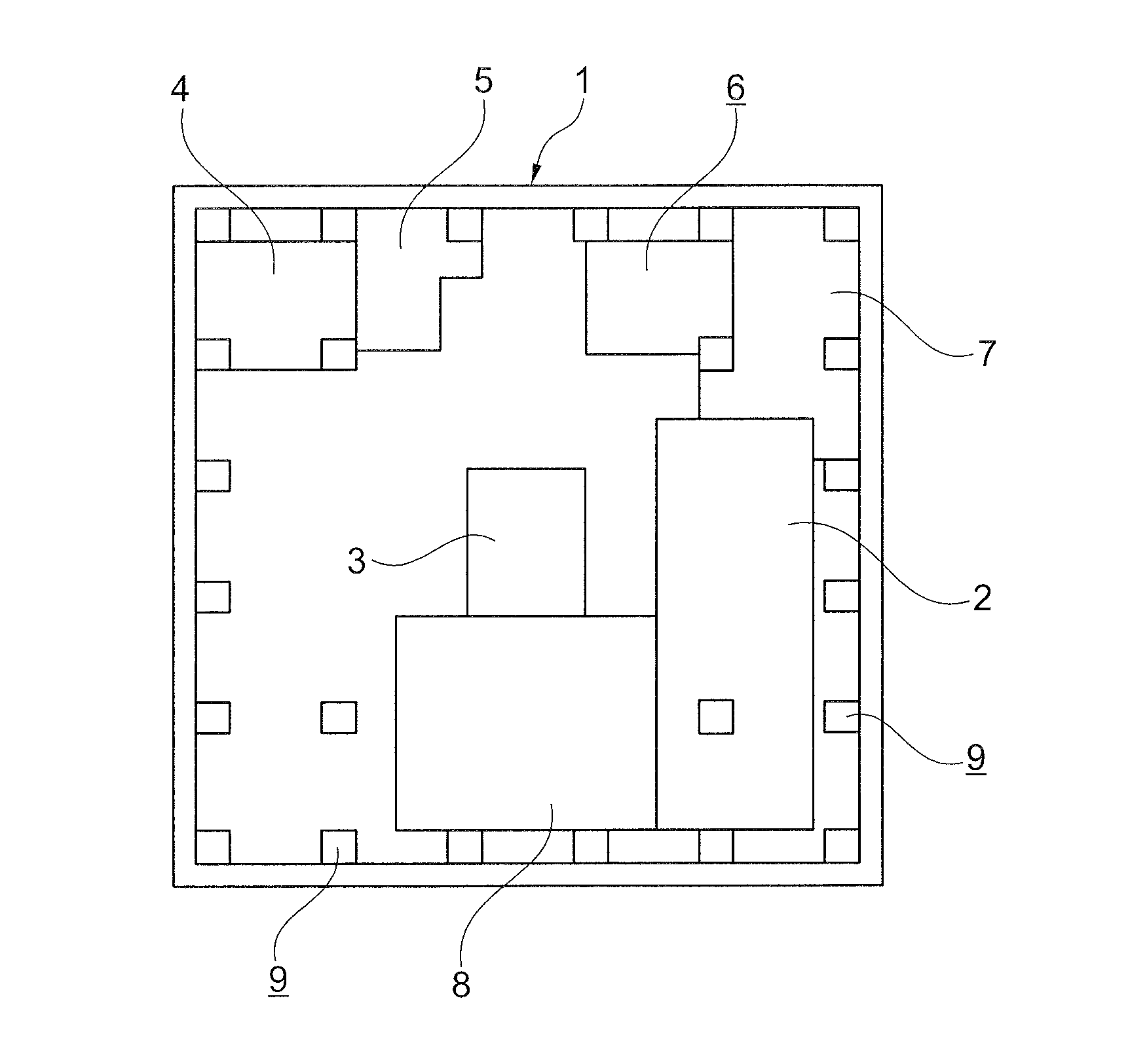
[0050]FIG. 1 shows a schematic illustration of a plan view of a sensor apparatus 1 according to the invention, which is embodied as a fully integrated system-on-chip. The entire chip 1, as is illustrated in FIG. 1, has a size of 2.55 mm×2.55 mm (where: mm: abbreviation of millimeter). Specifically, only the regions in which essential modules are arranged are illustrated; other electronics, conductor tracks or the like, which may be illustrated in specific detail only with difficulty anyway in the size of the drawing, have been omitted in FIG. 1. The schematically illustrated component mounting plan shows, inter alia, the following modules and circuit components, namely the digital domain 2 for signal processing, the pixel matrix 3 for detection, the voltage converter (charge pump) 4, the driver for the light emitting diode (LED) 5, the EEPROM 6 for storing configuration parameters, a module 7 comprising both a resonant circuit (PLL, phase-locked loop) and an apparatus for measuring ...


PUM


Abstract

A sensor apparatus including at least one analog and one digital circuit component and an analog/digital converter for converting analog signals of the analog circuit component into digital signals for the digital circuit component, and vice versa, wherein the analog circuit component and the digital circuit components include at least one module for electronically implementing a function, and wherein one of the modules of the analog circuit component is embodied as a sensor device for detecting optical radiation and one of the modules of the digital circuit component is embodied as a signal processing device for processing digital signals. In order to enable improved integration into application-based sensor devices, the circuit components including the analog/digital converter are integrated as an integrated circuit in a chip and the chip is manufactured as a semiconductor structure using 1-poly technology.

Description

FIELD OF THE INVENTION[0001]The invention relates to a sensor apparatus, in particular a time-of-flight (TOF) and / or CCD sensor apparatus for a 3-D camera sensor, a method for producing the sensor apparatus, and a detection apparatus.BACKGROUND OF THE INVENTION[0002]While on the one hand there is a general trend toward ever greater miniaturizations in the chip design, on the other hand many chips and optoelectronic sensor apparatuses can only be used to a very limited extent and have to be implemented in some instances in a complex manner with provision of some peripherals in cameras or other sensor devices. Difficulties can occur, in particular, because corresponding sensor devices are too large and too complex, but often the necessary robustness is also lacking with respect to the application-related requirements.SUMMARY OF THE INVENTION[0003]It is an object of the invention to propose a sensor apparatus and a method for producing it which enables improved integration into applica...

Claims


Application Information

Patent Timeline
IPC IPC(8): H01J40/14H01L31/18B82Y20/00G01S7/4863G01S17/894
CPCG01S17/36G01S7/4863G01S17/89G01S17/894
Inventor POPP, MARTINDE COI, BEAT
Owner ESPROS PHOTONICS
Why Eureka
Try Eureka