Method for Manufacturing a Flexible Electronic Device Using a Roll-Shaped Motherboard, Flexible Electronic Device, and Flexible Substrate

a technology of flexible electronic devices and roll-shaped motherboards, applied in the direction of final product manufacturing, solid-state devices, resistive material coatings, etc., can solve the problems of weak interfacial bonding strength, degrading yield, and devices that cannot be manufactured using plastic substrates, etc., to achieve the manufacture of high-performance flexible electronic devices, low cost, and easy-to-reach

Inactive Publication Date: 2013-07-25
POHANG IRON & STEEL CO LTD
View PDF249 Cites 33 Cited by
  • Summary
  • Abstract
  • Description
  • Claims
  • Application Information

AI Technical Summary

Benefits of technology

[0040]A flexible electronic device manufacturing method, a flexible electronic device, and a flexible substrate, according to the present invention, can bring about the following effects, and are thus expected to contribute to manufacturing of high-performance flexible electronic devices at low cost.
[0041]First, by forming an electronic device on a separation surface having substantially the same surface roughness as a roll-type mother substrate, the problem of surface roughness of a flexible substrate, particularly, a metal flexible substrate, which could not be solved by an existing method of manufacturing a flexible electronic device, can be easily solved.
[0042]Second, since surface roughness of a flexible substrate can be maintained at a very low level, a polymeric planarizing layer which decreases a processing temperature to 350° C. or less is not necessary. Therefore, process time and cost can be saved. Further, a high-performance electronic device such as a polysilicon TFT may be manufactured through a process of high temperature of 450° C. or above.
[0043]Third, to manufacture a flexible substrate, a high cost polishing process is not necessary, and a problem of low yield due to high defect density can be solved, thereby improving economic feasibility.
[0044]Fourth, in the case of using an INVAR alloy for a flexible substrate of the present invention, a thermal expansion coefficient may be adjusted to a similar level in comparison with an inorganic semiconductor such as Si, SiO2, and SiN and insulator. Therefore, it is not necessary to change a process condition such as a temperature increase rate or a temperature decrease rate, thereby reducing cracks caused by a thermal expansion coefficient difference.
[0045]Fifth, according to the flexible electronic device manufacturing method of the present invention, in which a temporary substrate for supporting a flexible substrate is used, an existing glass substrate process and existing equipment can be used without experiencing problems of bending, transporting, and alignment of a substrate, thereby facilitating a handling operation.

Problems solved by technology

In particular, it has become an important issue to develop a technology for manufacturing active matrix OLEDs (AMOLEDs), a display having the highest possibility of being made flexible and having excellent characteristics, at a high yield rate using an existing polysilicon TFT process.
Therefore, these devices cannot be manufactured using plastic substrates.
Further, during a manufacturing process, a defect such as a crack or exfoliation occurs due to a thermal expansion coefficient difference between an inorganic semiconductor such as Si, SiO2, or SiN and plastic of an insulator and substrate, thereby degrading a yield.
According to this method, since the temporary substrate is bonded on the thin-film device and then is separated therefrom, interfacial bonding strength is weak, and this method cannot be applied to an organic electronic device such as an OLED that is vulnerable to moisture or solvent.
Further, during processes of bonding and removing the glass substrate and the temporary substrate, the thin-film device may crack and impurities may be mixed, thereby degrading a yield.
Thus, it is difficult to manufacture a flexible metal substrate having low surface roughness.
However, in the case of decreasing surface roughness by using polymeric materials, a high temperature process cannot be performed as mentioned above with respect to a plastic substrate process.
A polishing process may be appropriate for a high-priced microprocessor or RAM using a single crystal Si substrate, but is not appropriate for a flexible electronic device requiring a large area in terms of economic feasibility.

Method used


Image

  • Method for Manufacturing a Flexible Electronic Device Using a Roll-Shaped Motherboard, Flexible Electronic Device, and Flexible Substrate
  • Method for Manufacturing a Flexible Electronic Device Using a Roll-Shaped Motherboard, Flexible Electronic Device, and Flexible Substrate
  • Method for Manufacturing a Flexible Electronic Device Using a Roll-Shaped Motherboard, Flexible Electronic Device, and Flexible Substrate

Examples


second embodiment

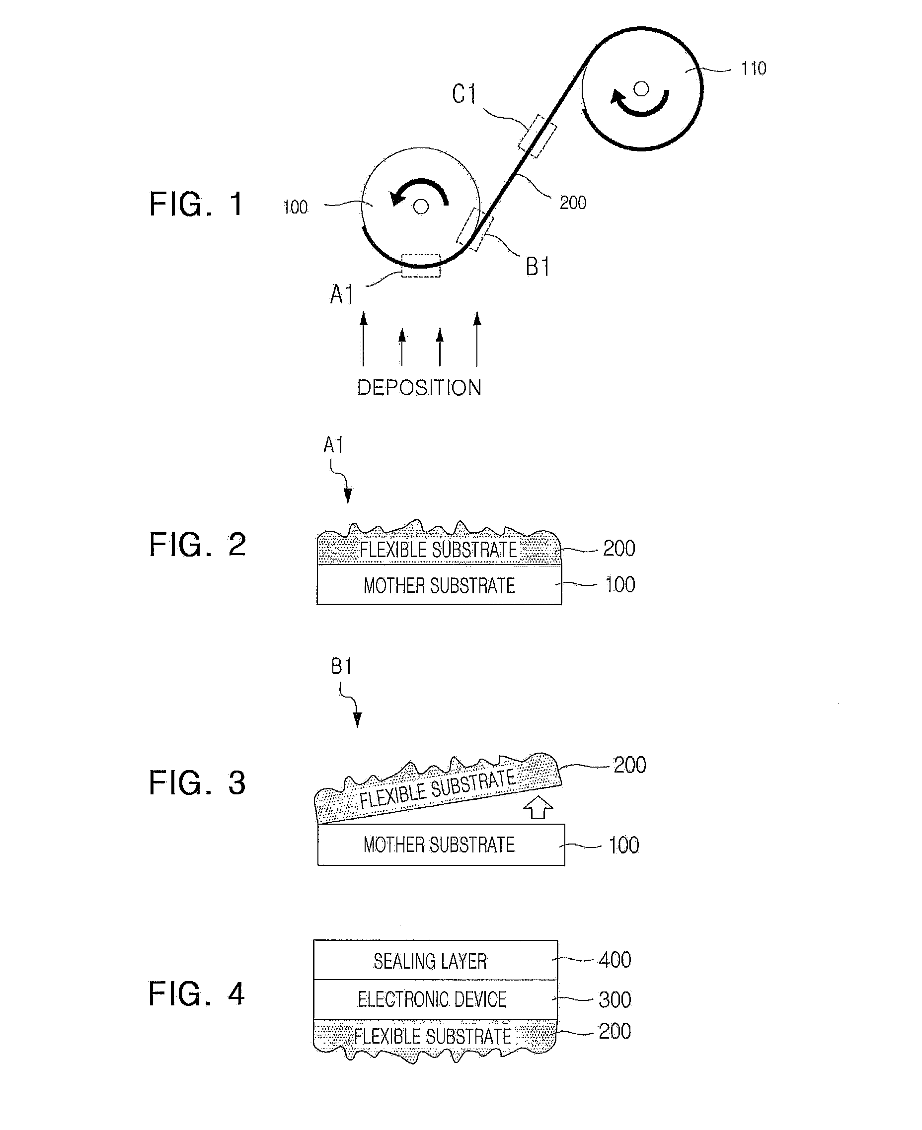
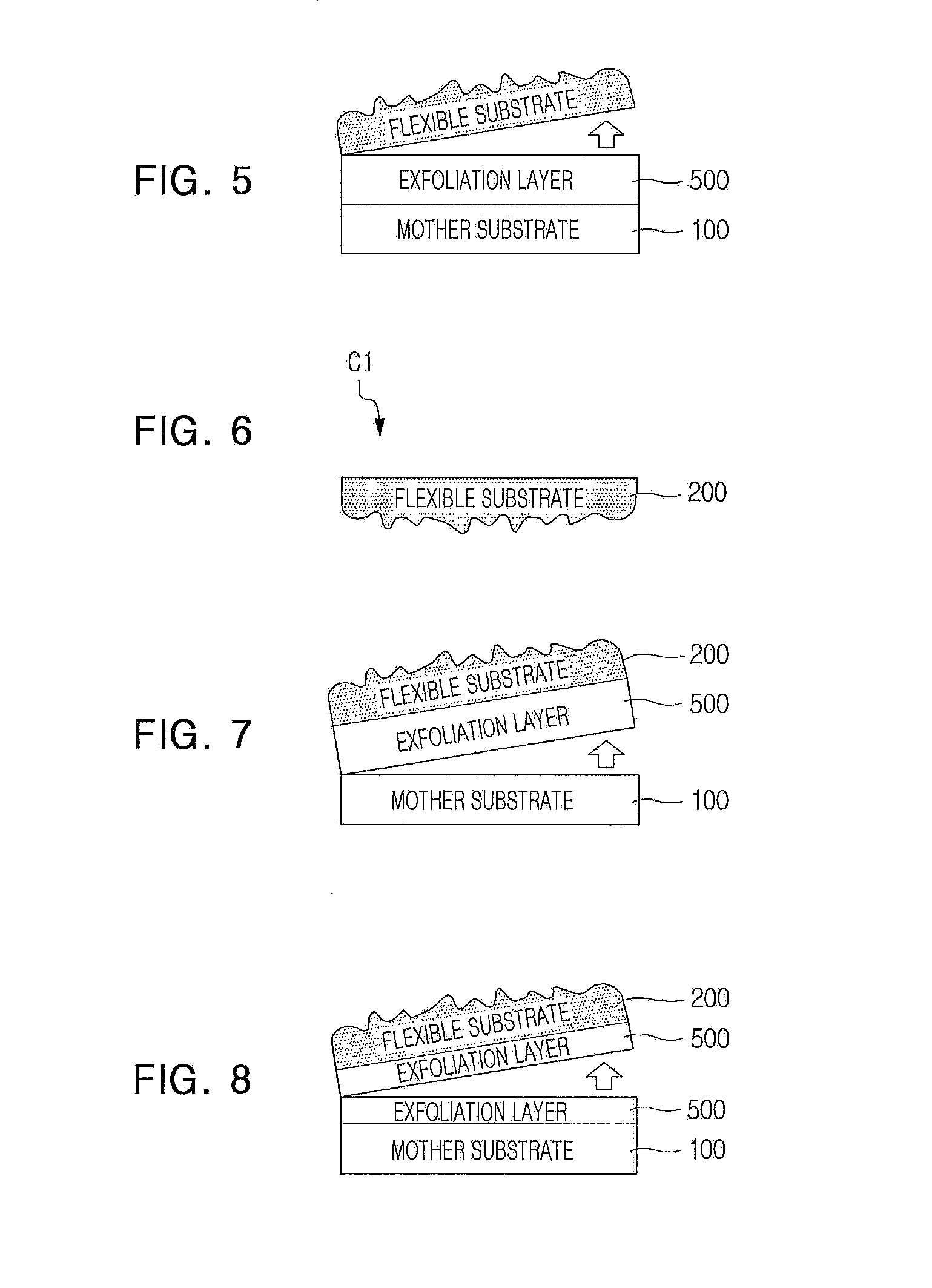
[0059]As illustrated in FIGS. 6 to 8, in a second embodiment of the present invention, an exfoliation layer 500 is formed between the roll-type substrate 100 and the flexible substrate 200 to manufacture the flexible substrate 200. In the case of forming the exfoliation layer 500, the flexible substrate 200 may be separated at an interface of the substrate 200 as illustrated in FIG. 6, may be separated at an interface between the roll-type mother substrate 100 and the exfoliation layer 500 as illustrated in FIG. 7, or may be separated at an inner side of the exfoliation layer 500 as illustrated in FIG. 8. Here, in the case of FIG. 6, an additional process may not be necessary. However, in the case of FIGS. 7 and 8, a process of removing the exfoliation 500 may be added.

[0060]In the second embodiment of the present invention, similarly to the first embodiment, the roll-type mother substrate 100 is physically separated from the flexible substrate 200 by using low interfacial bonding s...

third embodiment

[0062]FIGS. 9 to 14 are schematic diagrams illustrating a method of manufacturing a flexible electronic device according to a third embodiment of the present invention.

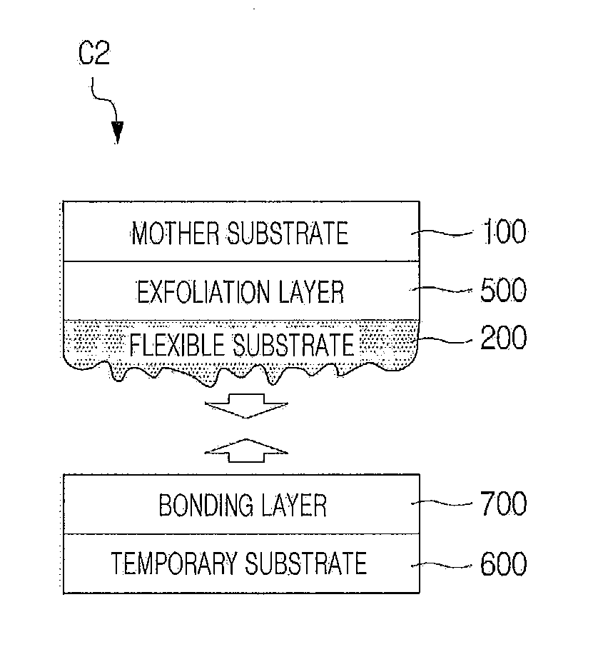
[0063]Referring to FIGS. 9 to 14, in the method of manufacturing a flexible electronic device, according to the third embodiment of the present invention, the flexible substrate 200 is deposited on the roll-type mother substrate 100 (A2 of FIG. 9 and FIG. 10), and then a bonding layer 700 is interposed thereon to bond a temporary substrate 600 to the flexible substrate 200 (B2 of FIG. 9 and FIGS. 11, and C2 of FIG. 9 and FIG. 12). Thereafter, the roll-type mother substrate 100 is separated from the flexible substrate 200 (D2 of FIG. 9 and FIG. 13), and an electronic device 300 and sealing layer 400 are formed on a separation surface of the flexible substrate 200 to manufacture a flexible electronic device (E2 of FIG. 9 and FIG. 14).

[0064]That is, the third embodiment is different from the first embodiment in that the ...


PUM

PropertyMeasurementUnit
surface roughnessaaaaaaaaaa
temperatureaaaaaaaaaa
thicknessaaaaaaaaaa

Abstract

A method of manufacturing a flexible electronic device includes forming a flexible substrate on a roll-type mother substrate, separating the flexible substrate from the roll-type mother substrate, and forming an electronic device on a separation surface of the flexible substrate, which has contacted the roll-type mother substrate, thus solving the problems of low performance and low yield of flexible electronic devices due to a low processing temperature, high surface roughness, high thermal expansion coefficient, and poor handling characteristics.

Description

TECHNICAL FIELD[0001]The present invention relates to a method of manufacturing a flexible electronic device, a flexible electronic device manufactured by the method, and a flexible substrate used for a flexible electronic device, and more particularly, to a flexible electronic device including a flexible substrate having a novel structure which allows for a high processing temperature at the same level as a glass substrate and has low surface roughness, a low thermal expansion coefficient, and excellent handling characteristics, and a method of manufacturing the same.BACKGROUND ART[0002]With the development of multimedia, flexible electronic devices are becoming more important. Accordingly, it is necessary to manufacture organic light emitting displays (OLEDs), liquid crystal displays (LCDs), electrophoretic displays (EPDs), plasma display panels (PDPs), thin-film transistors (TFTs), microprocessors, and random access memories (RAMs) on flexible substrates.[0003]In particular, it h...

Claims


Application Information

Patent Timeline
Patent Type & Authority Applications(United States)
IPC IPC(8): H05K1/02
CPCG02F1/133305H01L27/1218H01L27/1266H01L29/78603H05K1/0277H01L51/003Y02E10/549Y02P70/50H10K71/80H10K77/111
Inventor LEE, JONG LAMKIM, KEE SOO
Owner POHANG IRON & STEEL CO LTD
Why Eureka
Try Eureka