Dual metal fill and dual threshold voltage for replacement gate metal devices

Inactive Publication Date: 2013-08-08
APPLIED MATERIALS INC +1
View PDF4 Cites 36 Cited by
  • Summary
  • Abstract
  • Description
  • Claims
  • Application Information

AI Technical Summary

Benefits of technology

[0008]In another embodiment, a semiconductor structure is provided. The semiconductor structure comprises a first field effect transistor comprising a first gate cavity, a se

Problems solved by technology

However, this technique often requires additional mask levels, resulting in higher complexity and cost for fabrication.
Furt

Method used


Image

  • Dual metal fill and dual threshold voltage for replacement gate metal devices
  • Dual metal fill and dual threshold voltage for replacement gate metal devices
  • Dual metal fill and dual threshold voltage for replacement gate metal devices

Examples


Embodiment Construction

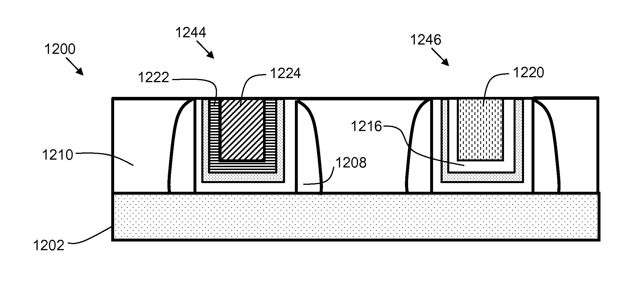
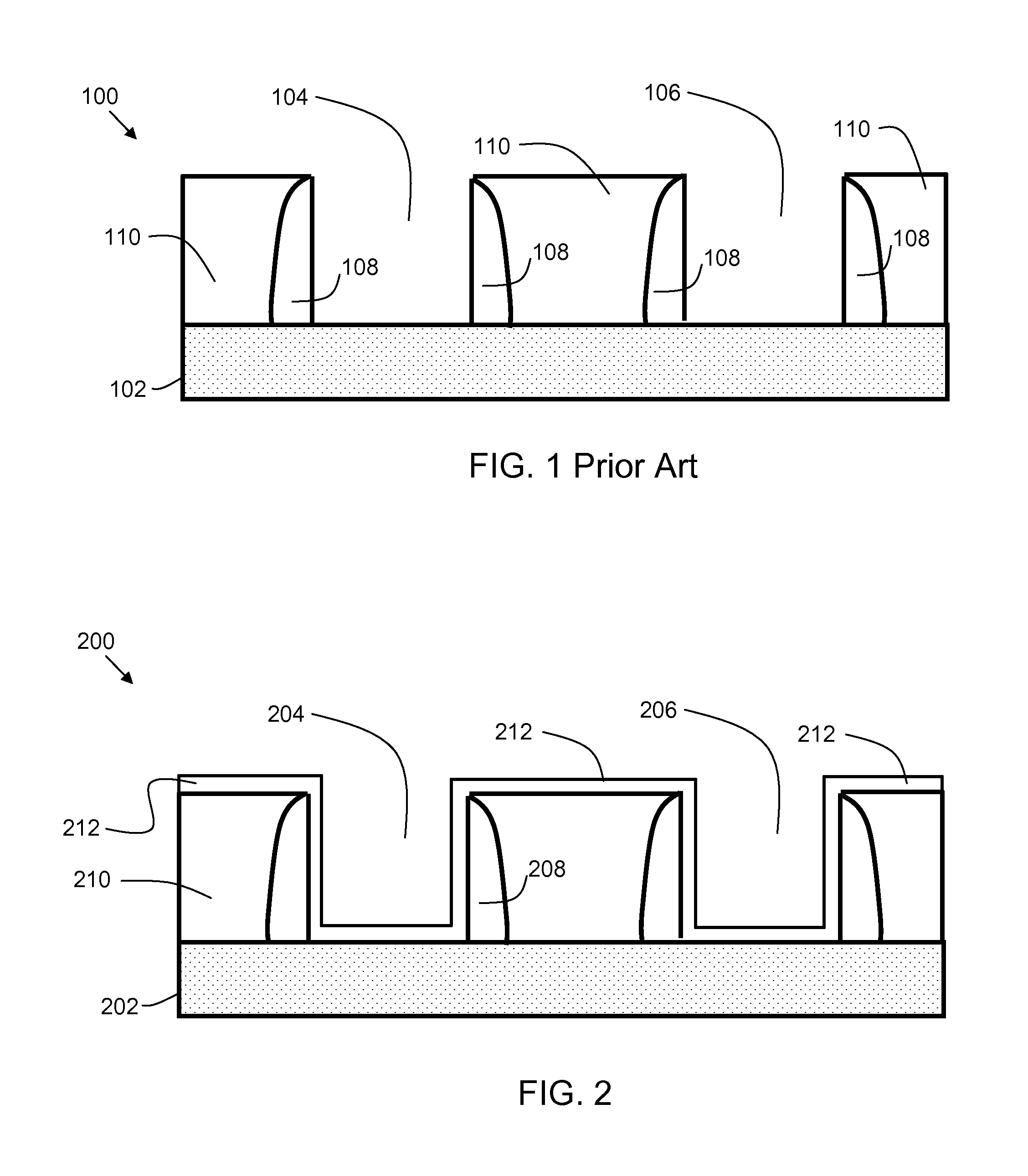
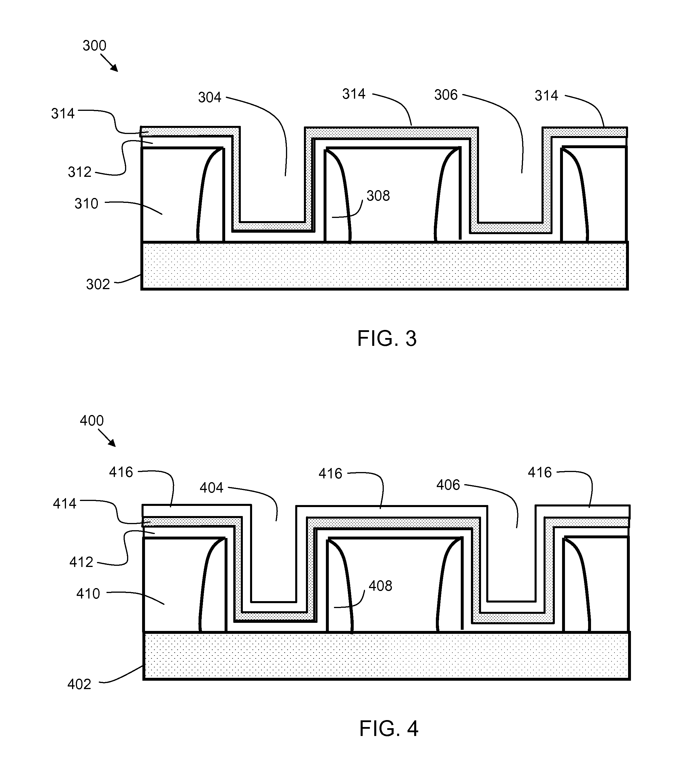
[0026]FIG. 1 shows a semiconductor structure at a starting point for fabrication of an embodiment of the present invention. A silicon layer 102 forms the bottom of the structure. Disposed on silicon layer 102 is dielectric layer 110. A first gate cavity 106 and second gate cavity 104 are formed within the dielectric layer 110. Spacers 108 form the interior walls of the gate cavity 104 and gate cavity 106. The spacers 108 may be comprised of nitride.

[0027]FIG. 2 shows a semiconductor structure 200 at a subsequent point in the fabrication process where gate dielectric film 212 is deposited in the first gate cavity 206 and second gate cavity 204. Most any suitable gate dielectric material can be used. In one embodiment, the gate dielectric film comprises one of hafnium oxide, silicon oxide, or a compound of the form HfSiOx. As stated previously, similar elements may be referred to by similar numbers in various figures of the drawing, in which case typically the last two significant dig...


PUM


Abstract

A structure and method for forming a dual metal fill and dual threshold voltage for replacement gate metal devices is disclosed. A selective deposition process involving titanium and aluminum is used to allow formation of two adjacent transistors with different fill metals and different workfunction metals, enabling different threshold voltages in the adjacent transistors.

Description

FIELD OF THE INVENTION[0001]The present invention relates generally to semiconductor devices and more particularly to integrated circuits including metal gate MOS transistor devices and fabrication methods for making the same.BACKGROUND OF THE INVENTION[0002]Field effect transistors (FETs) are widely used in the electronics industry for switching, amplification, filtering, and other tasks related to both analog and digital electrical signals. Most common among these are metal-oxide-semiconductor field-effect transistors (MOSFETs), wherein a gate electrode is energized to create an electric field in a channel region of a semiconductor body, by which electrons are allowed to travel through the channel between a source region and a drain region of the semiconductor body. The source and drain regions are typically formed by adding dopants to targeted regions on either side of the channel. A gate dielectric or gate oxide is formed over the channel, and a gate electrode or gate contact is...

Claims


Application Information

Patent Timeline
IPC IPC(8): H01L27/088H01L21/28
CPCH01L21/82345H01L21/823842H01L29/49H01L29/66545H01L27/088H01L21/28088
Inventor EDGE, LISA F.BERLINER, NATHANIELDEMAREST, JAMES JOHNHARAN, BALASUBRAMANIAN S.
Owner APPLIED MATERIALS INC
Why Eureka
Try Eureka