Method for achieving sustained anisotropic crystal growth on the surface of a melt

a melt surface and anisotropic crystal technology, applied in the direction of crystal growth process, polycrystalline material growth, chemistry apparatus and processes, etc., can solve the problems of affecting the ability to obtain thin solar cells, the wafer on which the solar cell is mounted, and the efficiency of the solar cell, etc., to achieve the effect of reducing the cost of crystalline silicon solar cells

Inactive Publication Date: 2013-08-22
VARIAN SEMICON EQUIP ASSOC INC
View PDF2 Cites 10 Cited by
  • Summary
  • Abstract
  • Description
  • Claims
  • Application Information

AI Technical Summary

Benefits of technology

[0009]This Summary is provided to introduce a selection of concepts in a simplified form that are further described below in the Detailed Description. This Summary is not intended to identify key features or essential features of the claimed subject matter, nor is it intended as an aid in determining the scope of the claimed subject matter.

Problems solved by technology

Currently, a major cost of a crystalline silicon solar cell is the wafer on which the solar cell is made.
The efficiency of the solar cell, or the amount of power produced under standard illumination, is limited, in part, by the quality of this wafer.
Limits inherent in ingot slicing technology, however, may hinder the ability to obtain thinner solar cells.
This results in a large temperature gradient along the ribbon.
This temperature gradient stresses the crystalline silicon ribbon and may result in poor quality multi-grain silicon.
The width and thickness of the ribbon also may be limited due to this temperature gradient.
These early attempts have not met the goal of producing a reliable and rapidly drawn wide ribbon with uniform thickness that is “production worthy”.

Method used


Image

  • Method for achieving sustained anisotropic crystal growth on the surface of a melt
  • Method for achieving sustained anisotropic crystal growth on the surface of a melt
  • Method for achieving sustained anisotropic crystal growth on the surface of a melt

Examples


Embodiment Construction

[0021]The present invention will now be described more fully hereinafter with reference to the accompanying drawings, in which preferred embodiments of the invention are shown. This invention, however, may be embodied in many different forms and should not be construed as limited to the embodiments set forth herein. Rather, these embodiments are provided so that this disclosure will be thorough and complete, and will fully convey the scope of the invention to those skilled in the art. In the drawings, like numbers refer to like elements throughout.

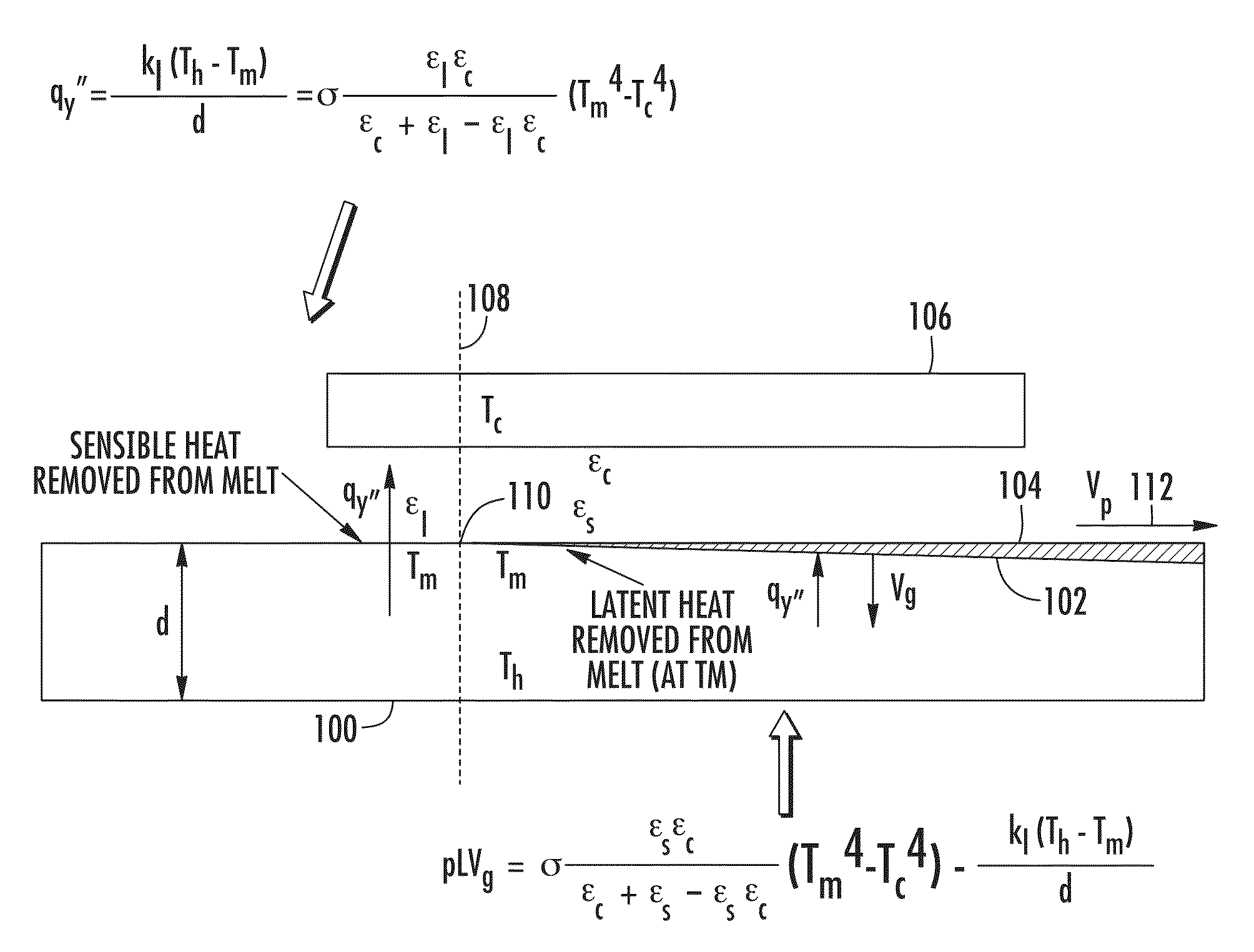
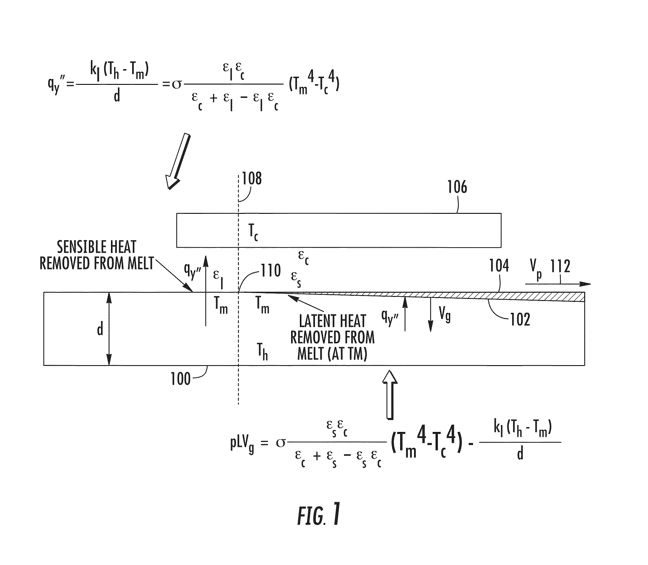
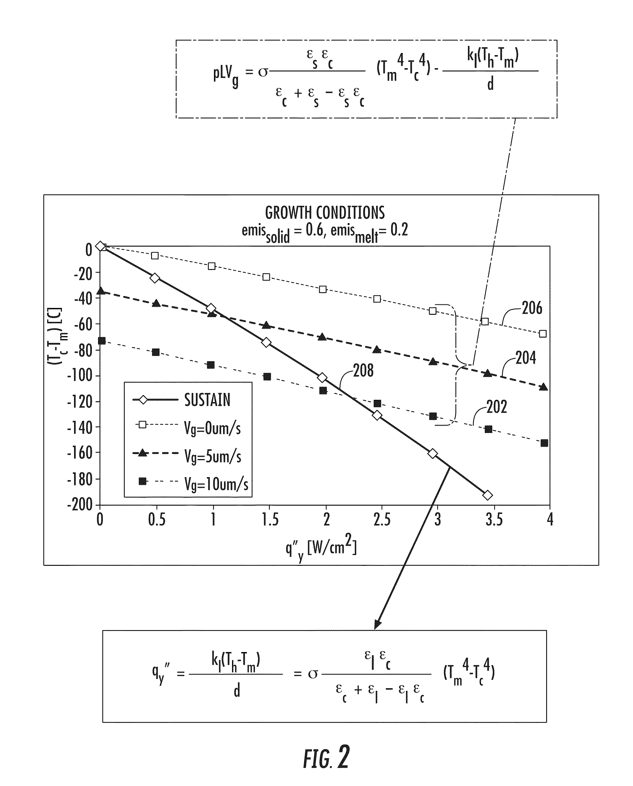
[0022]To solve the deficiencies associated with the methods noted above, the present embodiments provide novel and inventive techniques and systems for horizontal melt growth of a crystalline material, in particular, a monocrystalline material. In various embodiments, methods for forming a sheet of monocrystalline silicon by horizontal melt growth are disclosed. However, in other embodiments, the methods disclosed herein may be applied to ...


PUM

PropertyMeasurementUnit
emissivityaaaaaaaaaa
Tmaaaaaaaaaa

Abstract

A method of horizontal ribbon growth from a melt includes forming a leading edge of the ribbon using radiative cooling on a surface of the melt, drawing the ribbon in a first direction along the surface of the melt, and removing heat radiated from the melt in a region adjacent the leading edge of the ribbon at a heat removal rate that is greater than a heat flow through the melt into the ribbon.

Description

STATEMENT AS TO FEDERALLY SPONSORED RESEARCH OR DEVELOPMENT [0001]The U.S. Government has a paid-up license in this invention and the right in limited circumstances to require the patent owner to license others on reasonable terms as provided for by the terms of contract number DE-EE0000595 awarded by the U.S. Department of Energy.BACKGROUND OF THE INVENTION[0002]1. Field of the Invention[0003]Embodiments of the invention relate to the field of substrate manufacturing. More particularly, the present invention relates to a method, system and structure for removing heat from a ribbon on a surface of a melt.[0004]2. Discussion of Related Art[0005]Silicon wafers or sheets may be used in, for example, the integrated circuit or solar cell industry. Demand for solar cells continues to increase as the demand for renewable energy sources increases. As these demands increase, one goal of the solar cell industry is to lower the cost / power ratio. There are two types of solar cells: silicon and ...

Claims


Application Information

Patent Timeline
Patent Type & Authority Applications(United States)
IPC IPC(8): C30B13/00
CPCC30B15/002C30B15/06C30B29/06C30B15/14
Inventor KELLERMAN, PETER L.SUN, DAWEIMACKINTOSH, BRIAN H.
Owner VARIAN SEMICON EQUIP ASSOC INC
Why Eureka
Try Eureka