
Visible and near-infrared radiation detector

Active Publication Date: 2013-08-22
COMMISSARIAT A LENERGIE ATOMIQUE ET AUX ENERGIES ALTERNATIVES
View PDF3 Cites 23 Cited by
  • Summary
  • Abstract
  • Description
  • Claims
  • Application Information

AI Technical Summary

Benefits of technology

The patent text is looking for a detector that can see both visible and near-infrared light. It should be easy to make and very good at picking up on color.

Problems solved by technology

In night vision or for a low lighting level, the amount of visible light (wavelength from 0.4 μm to 0.7 μm) is generally insufficient to perform a conventional image capture.
Its use as a near-infrared detection material is thus limited.
However, the performances are lower than those of silicon.
InGaAs is thus not optimized for visible detection.
Such a sensor is complex to produce.
In particular, the forming of an InGaAs / Si heterojunction to detect near-infrared radiation is difficult to control.
Further, the delimitation of the heterojunction by etching generates significant leakage currents.
This visible and near-infrared sensor has a poor performance.
Furthermore, this sensor does not enable to obtain a good color rendering.

Method used


Image

  • Visible and near-infrared radiation detector
  • Visible and near-infrared radiation detector
  • Visible and near-infrared radiation detector

Examples


first embodiment

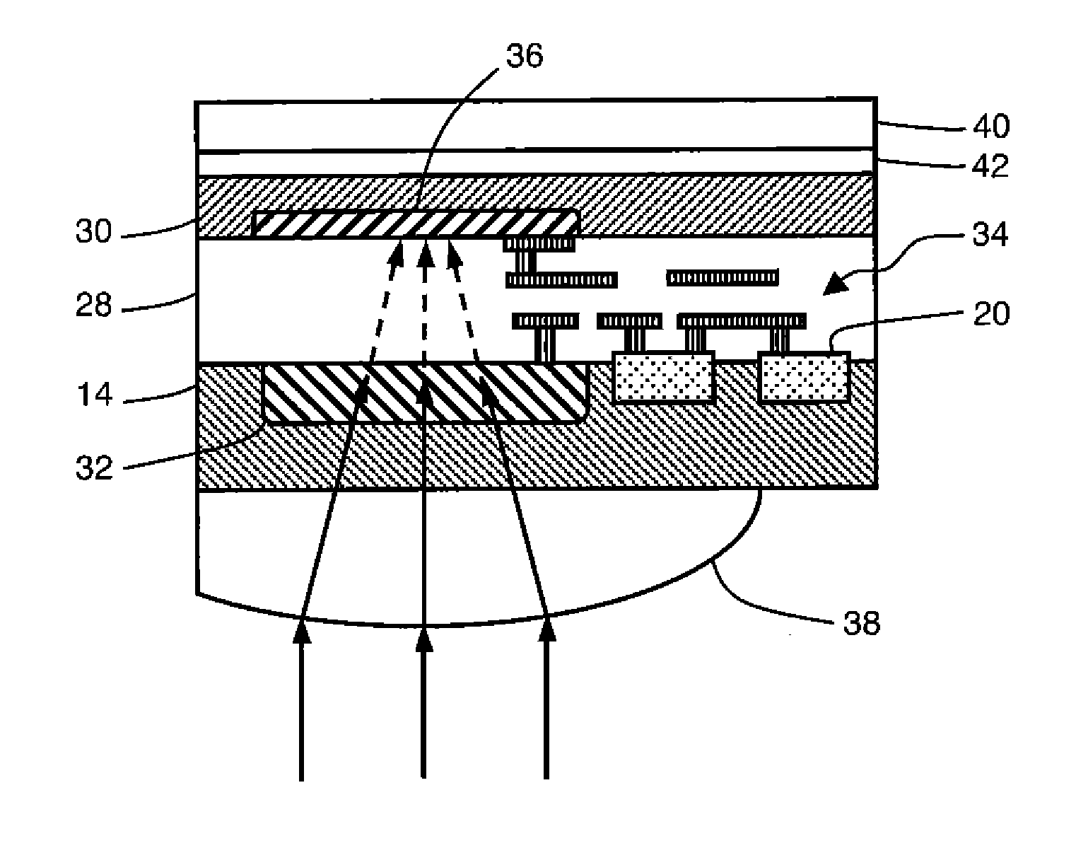
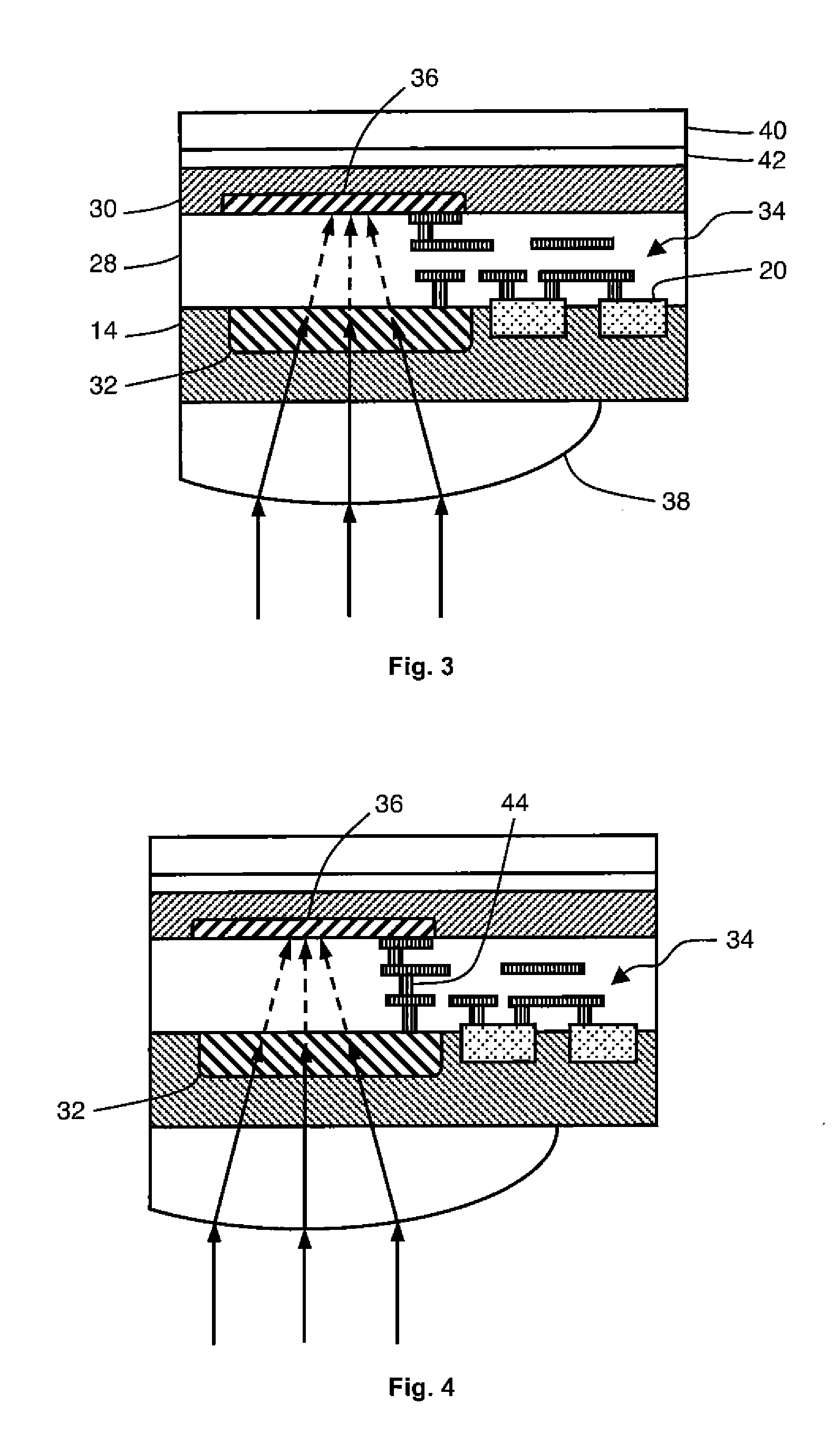
[0038]FIG. 3 schematically represents a detector of visible and near-infrared radiation. The detector successively comprises a silicon substrate 14, an interconnect layer 28, and a substrate 30 comprising at least one layer optimized for the detection of near-infrared radiation.

[0039]Silicon substrate 14 comprises a photodiode 32 and transistors 20. Transistors 20 are formed on a frontside of substrate 14 and covered with interconnect layer 28. Layer 28 is formed of metal tracks embedded in a dielectric material transparent to infrared radiation, for example, an oxide layer of PSG type (PSG, “Phosphosilicate glass”). The metal tracks interconnect transistors 20 and electrically connect them to photodiode 32 to form a readout circuit 34 of photodiode 32.

[0040]Substrate 30 preferably comprises a stack of layers made of materials sensitive to near-infrared to form a photodiode 36. The stack for example comprises an n-type doped InP layer, an intrinsic InGaAs absorption layer, and a p-t...

second embodiment

[0054]FIG. 6 represents a visible and near-infrared radiation detector enabling to obtain color in the visible spectrum. The detector comprises a pixel quadruplet. A first pixel 46 comprises a visible photodiode 32, a NIR photodiode 36, and a readout circuit 34. Pixel 46 thus corresponds to the detector of FIG. 3 or 4. The three other pixels 48a, 48b, and 48c each comprise a visible photodiode 32 and an associated readout circuit 34. Pixels 48a, 48b, and 48c are respectively provided with filters 50a-50c associated with the three elementary colors, for example, red (50a), blue (50b), and green (50c). Color filters 50a-50c are arranged between the incident radiation and photodiodes 32, on the backside of substrate 14.

[0055]In a conventional silicon color imager, the filter at the level of each pixel is generally made of a pigmented resin. This type of filter transmits part of the visible radiation but also a significant part of the near-infrared radiation to which silicon photodiodes...


PUM


Abstract

The visible and near-infrared radiation detector includes a near-infrared photosensitive element, a readout circuit for reading the near-infrared photosensitive element, four visible photosensitive elements, one of which being placed facing the near-infrared photosensitive element, and three interference filters to define a pixel quadruplet. A first pixel, including the near-infrared photosensitive element and one of the visible photosensitive elements, has no filter. The three other pixels, respectively including the three other visible photosensitive elements, are respectively provided with filters associated with the three primary colors. Each interference filter includes an alternation of metal layers and of dielectric layers.

Description

BACKGROUND OF THE INVENTION[0001]The invention relates to low lighting level imaging, and more specifically to a detector of visible and near-infrared radiation.STATE OF THE ART[0002]In night vision or for a low lighting level, the amount of visible light (wavelength from 0.4 μm to 0.7 μm) is generally insufficient to perform a conventional image capture. A sensor having a spectral response extending beyond the visible spectrum is then used. Thus, the amount of captured light is increased, which enables to obtain a more detailed image.[0003]In other words, a detection material having a high sensitivity for wavelengths greater than 0.7 μm, that is, a material sensitive to infrared, and more specifically to near-infrared, is desired. By definition, the sensitivity of a sensor corresponds to the ratio of the output signal of the detector to the normalized incident light intensity. It is a function of the wavelength. Near-infrared approximately corresponds to the spectral range of wavel...

Claims


Application Information

Patent Timeline
IPC IPC(8): G01J5/20H01L31/18H01L27/146
CPCH01L27/14621H01L27/14634H01L27/14636H01L27/14647H01L27/14685H01L27/14641G01J5/20H01L27/14625H01L31/18H01L27/1464H01L27/1469
Inventor CAZAUX, YVONGIFFARD, BENOITHUGON, XAVIER
Owner COMMISSARIAT A LENERGIE ATOMIQUE ET AUX ENERGIES ALTERNATIVES
Learn More