Oxide semiconductor film and semiconductor device
a technology of semiconductor devices and oxide semiconductor films, which is applied in semiconductor devices, electric lighting sources, and electric light sources. it can solve the problems of reducing the electrical conductivity of the oxide semiconductor film might change, and the so as to achieve stable electric conductivity, high reliability of the semiconductor device, and more electrical stability
- Summary
- Abstract
- Description
- Claims
- Application Information
AI Technical Summary
Benefits of technology
Problems solved by technology
Method used
Image
Examples
embodiment 1
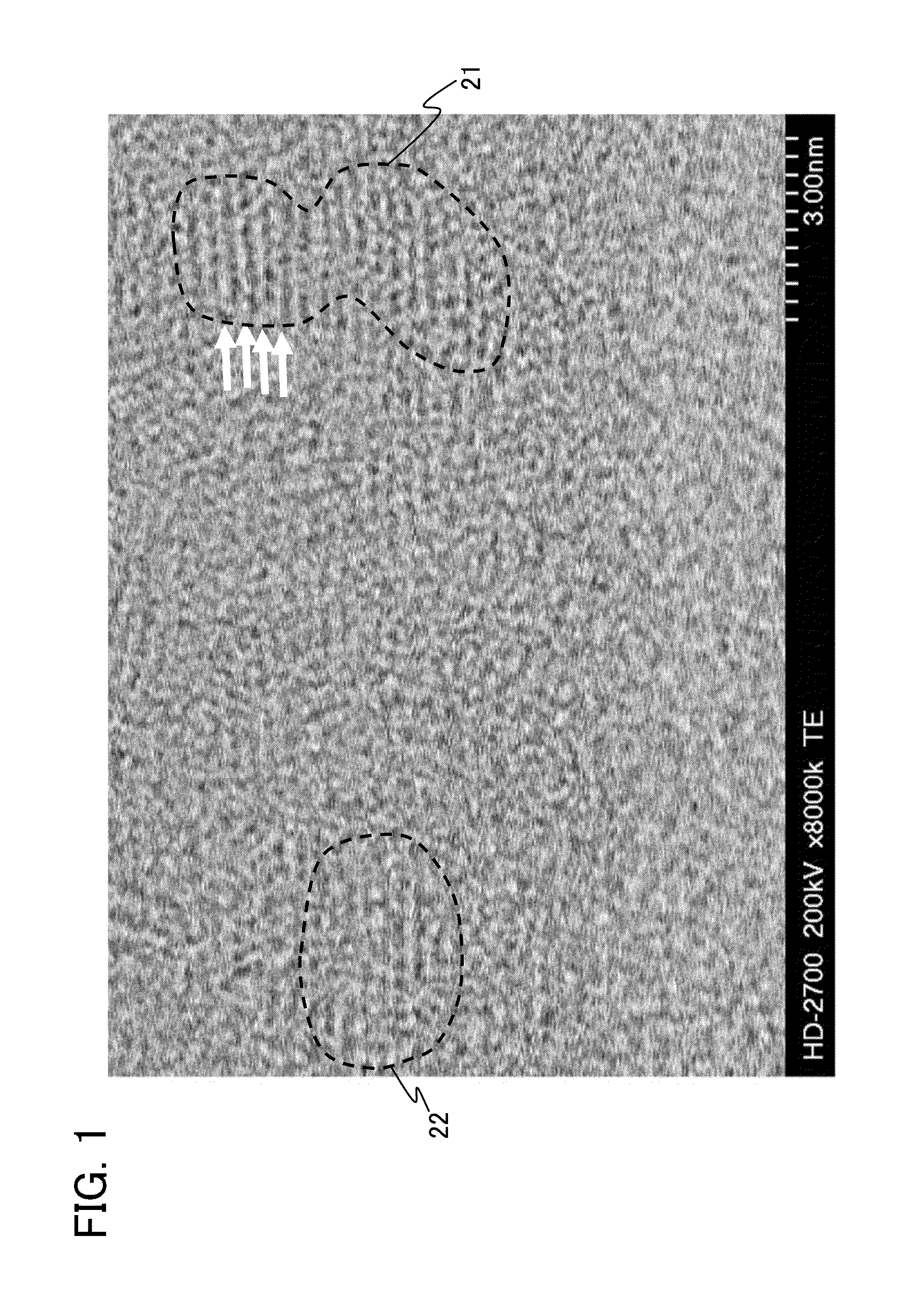
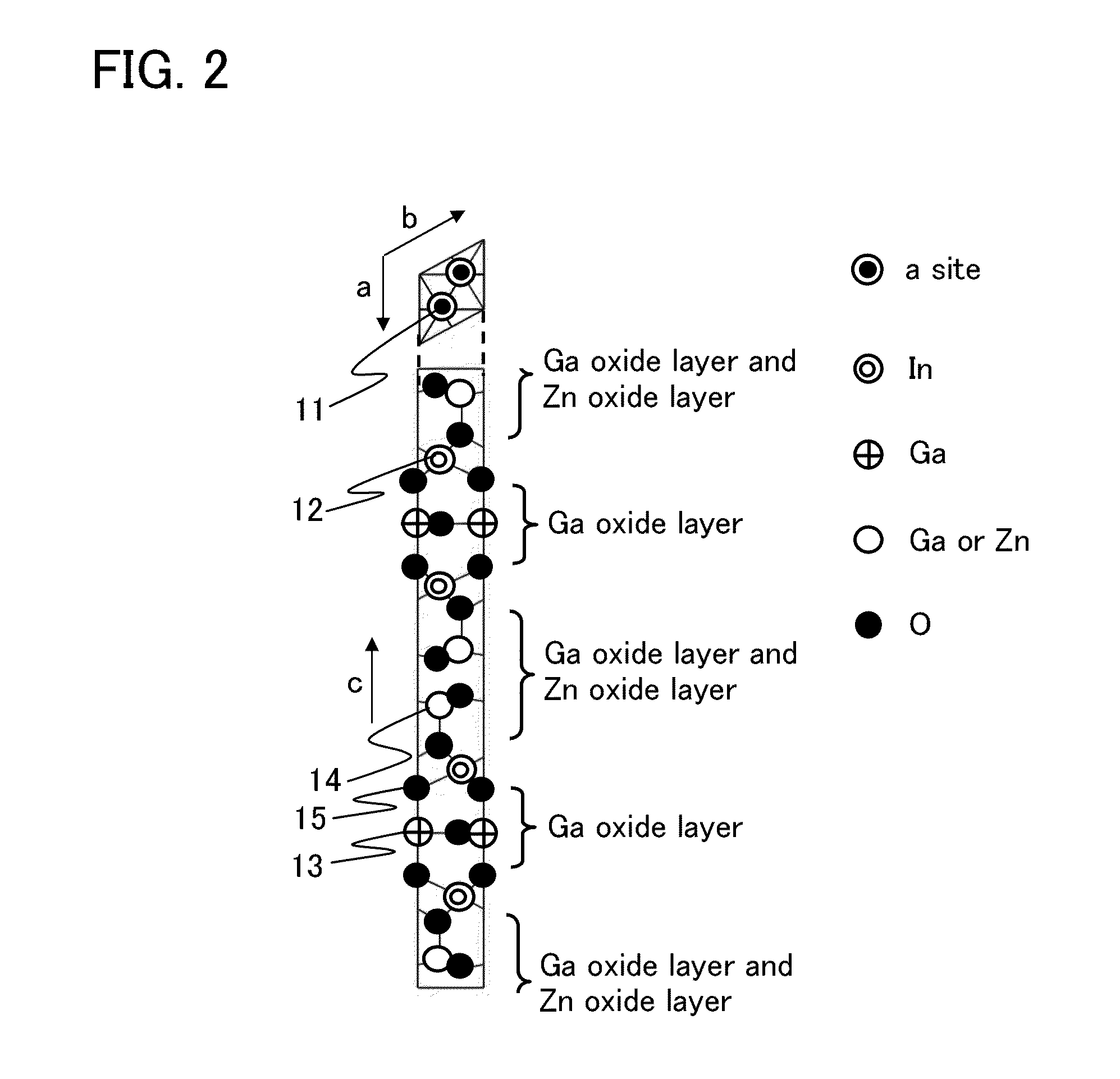
[0054]In this embodiment, an oxide semiconductor film will be described as an embodiment of the present invention with reference to FIG. 1, FIG. 2, FIG. 3, FIG. 4, and FIGS. 5A and 5B.
[0055]An oxide semiconductor film according to this embodiment includes a crystalline region. The crystalline region includes a crystal in which an a-b plane is substantially parallel with a surface of the film and a c-axis is substantially perpendicular to the surface of the film. That is, the crystalline region included in the oxide semiconductor film has c-axis alignment. When a cross section of the crystalline region is observed, atoms arranged in a layered manner and stacked from a substrate toward the surface of the film are observed, and the c-axis of the crystal is substantially perpendicular to the surface. Since the oxide semiconductor film includes the crystalline region with c-axis alignment as described above, the oxide semiconductor film is also referred to as a c-axis aligned crystalline...
embodiment 2
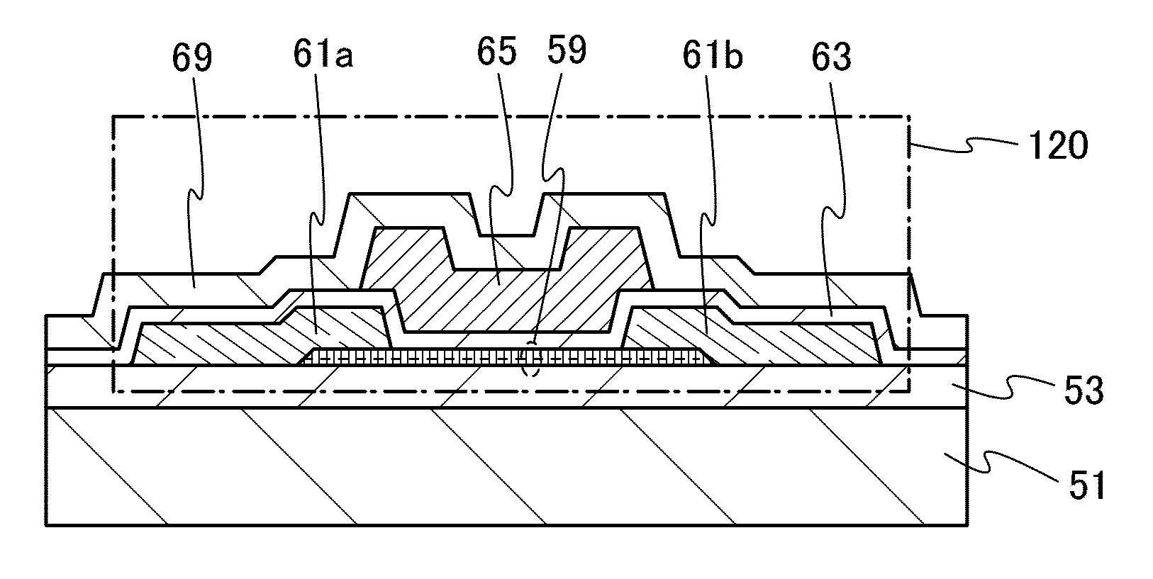
[0090]In this embodiment, a transistor in which the oxide semiconductor film including a crystalline region described in Embodiment 1 is used and a method for manufacturing the transistor will be described with reference to FIGS. 6A to 6E, FIGS. 7A and 7B, FIGS. 8A and 8B, FIGS. 9A and 9B, and FIGS. 10A to 10C. FIGS. 6A to 6E are cross-sectional views illustrating a manufacturing process of a top-gate transistor 120 which is an embodiment of the structure of a semiconductor device.
[0091]First, before an oxide semiconductor film including a crystalline region is formed, a base insulating film 53 is preferably formed over a substrate 51 as illustrated in FIG. 6A.
[0092]The substrate 51 should have at least heat resistance high enough to withstand heat treatment performed later. When a glass substrate is used as the substrate 51, a glass substrate whose strain point is higher than or equal to 730° C. is preferably used. As a glass substrate, a substrate formed of a glass material such a...
embodiment 3
[0167]In this embodiment, a transistor having a structure that is different from that of the transistor which includes the oxide semiconductor film including a crystalline region described in the above embodiment will be described with reference to FIGS. 11A to 11C and FIG. 12.
[0168]A transistor 160 having a top gate structure illustrated in FIG. 11A includes a base insulating film 353 provided over a substrate 351, a metal oxide film 371 provided over the base insulating film 353, an oxide semiconductor film 359 provided over the metal oxide film 371, a source electrode 361a and a drain electrode 361b provided in contact with an upper surface and side surfaces of the oxide semiconductor film 359, a metal oxide film 373 provided over the oxide semiconductor film 359, a gate insulating film 363 provided over the metal oxide film 373, a gate electrode 365 provided over the gate insulating film 363 so as to overlap with the oxide semiconductor film 359, and an insulating film 369 provi...
PUM
 Abstract
Description
Claims
Application Information


