Semiconductor light emitting diode having ohmic electrode structure and method of manufacturing the same

a technology of ohmic electrodes and semiconductors, applied in the direction of semiconductor/solid-state device manufacturing, semiconductor devices, electrical apparatus, etc., can solve the problems of increasing operating voltage, low thermal stability, and poor optical output of current nitride semiconductor light-emitting diodes, so as to reduce operating voltage characteristics, reduce operating voltage, and maintain thermal stability

Active Publication Date: 2013-08-29
SEOUL VIOSYS CO LTD +1
View PDF8 Cites 4 Cited by
  • Summary
  • Abstract
  • Description
  • Claims
  • Application Information

AI Technical Summary

Benefits of technology

[0025]Since the semiconductor light emitting diode according to the present invention employs a multilayered ohmic electrode structure including a lower diffusion preventing layer, a contact layer, an upper diffusion preventing layer, and an Al protective layer, the lower diffusion preventing layer mitigates deterioration of an N-face semiconductor. Further, an upper diffusion preventing layer is disposed between the contact layer and the protective layer so as to prevent diffusion of Al elements in the protective layer. Accordingly, since the contact layer acts as a diffusion barrier layer of a metal of the protective layer, deterioration of contact resistance due to nitrogen atmosphere heat treatment and heat generated under a high current injection condition such as for a high output light emitting diode can be restrained, making it possible to maintain thermal stability.
[0026]Further, according to the present invention, the semiconductor light emitting diode employs the multilayered ohmic electrode structure including a lower diffusion preventing layer, a contact layer, a diffusion preventing layer and an Al protective layer, and thus has lower operating voltage characteristics, thereby further improving operation reliability.

Problems solved by technology

However, current nitride semiconductor light emitting diodes are not satisfactory in terms of optical output, luminous efficacy, and price, and their performance needs to be further improved.
However, the horizontal light emitting diode employs a sapphire substrate, which is nonconductive and has poor thermal conductivity, it requires application of a large area current for realization of a high output and suffers from low thermal stability due to accumulation of heat.
However, in the ohmic electrode, ohmic characteristics deteriorate due to heat generated upon heat treatment for forming a SiO2 protective film after formation of the electrodes or upon application of high current to a large area light emitting diode, thereby causing increase in operating voltage.

Method used


Image

  • Semiconductor light emitting diode having ohmic electrode structure and method of manufacturing the same
  • Semiconductor light emitting diode having ohmic electrode structure and method of manufacturing the same
  • Semiconductor light emitting diode having ohmic electrode structure and method of manufacturing the same

Examples


Embodiment Construction

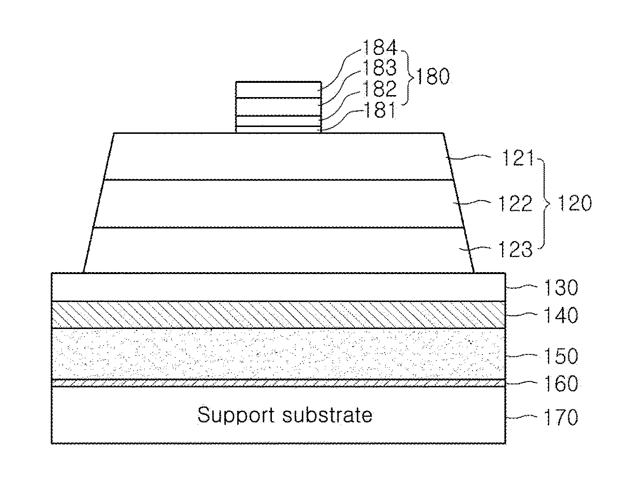
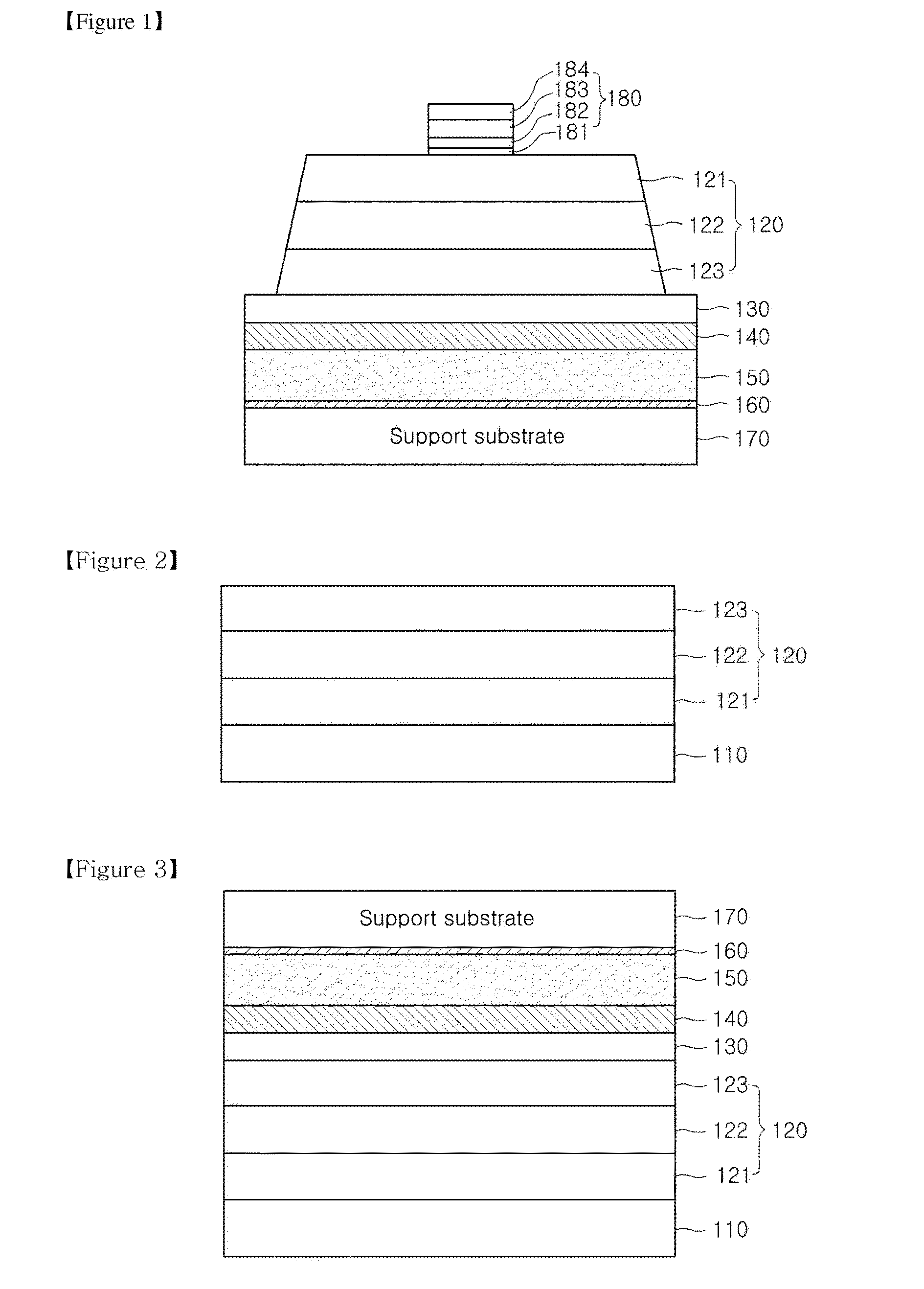
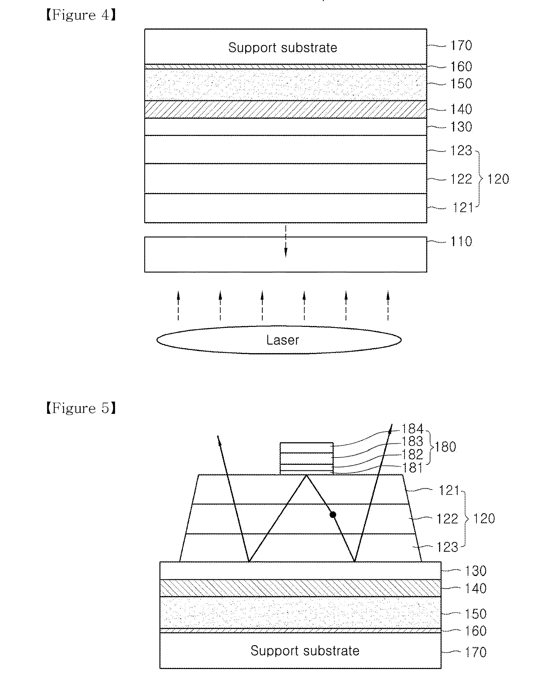
[0034]The invention is described more fully hereinafter with reference to the accompanying drawings, in which exemplary embodiments of the invention are shown. This invention may, however, be embodied in many different forms and should not be construed as limited to the exemplary embodiments set forth herein. Rather, these exemplary embodiments are provided so that this disclosure is thorough and will fully convey the scope of the invention to those skilled in the art. In the drawings, the sizes and relative sizes of layers and regions may be exaggerated for clarity. Like reference numerals in the drawings denote like elements. It will be understood that when an element such as a layer, film, region or substrate is referred to as being “on” another element, it can be directly on the other element or intervening elements may also be present. In contrast, when an element is referred to as being “directly on” another element, there are no intervening elements present.

[0035]FIG. 1 is a ...


PUM


Abstract

Embodiments of the invention provide a semiconductor light emitting diode having an ohmic electrode structure, and a method of manufacturing the same. The semiconductor light emitting diode includes a light emitting structure having an upper surface constituting an N-face; and an ohmic electrode structure located on the light emitting structure. Here, the ohmic electrode structure includes a lower diffusion preventing layer, a contact layer, an upper diffusion preventing layer, and an Al protective layer from the N-face of the light emitting structure.

Description

CROSS-REFERENCE TO RELATED APPLICATIONS[0001]This application is the National Stage Entry of International Application No. PCT / KR2011 / 005796, filed on Aug. 9, 2011 and claims priority from and the benefit of Korean Patent Application No. 10-2010-0078115, filed on Aug. 13, 2010, which are hereby incorporated by reference for all purposes as if fully set forth herein.BACKGROUND[0002]1. Field[0003]The present invention relates to a semiconductor light emitting diode and a method of manufacturing the same, and more particularly, to a semiconductor light emitting diode including an ohmic electrode structure on a semiconductor layer of a light emitting structure to connect an external power source and a method of manufacturing the same.[0004]2. Discussion of the Background[0005]A semiconductor light emitting diode (LED) has a long lifespan, is small and lightweight, shows strong directivity of light, and can be driven at low voltage. In addition, a semiconductor light emitting diode (LED)...

Claims


Application Information

Patent Timeline
Patent Type & Authority Applications(United States)
IPC IPC(8): H01L33/40
CPCH01L33/0095H01L33/32H01L33/40H01L2933/0016H01L33/405
Inventor LEE, JONG LAMSONG, YANG HEE
Owner SEOUL VIOSYS CO LTD
Why Eureka
Try Eureka