Devices and methods related to interconnect conductors to reduce de-lamination

Active Publication Date: 2013-08-29
SKYWORKS SOLUTIONS INC
View PDF8 Cites 0 Cited by
  • Summary
  • Abstract
  • Description
  • Claims
  • Application Information

AI Technical Summary

Benefits of technology

The present disclosure involves a device having a die with an intrinsic region and a metal layer in ohmic contact with the intrinsic region. A passivation layer is formed over the metal layer and the intrinsic region with an opening exposing at least a portion of the metal layer. An interconnect conductor is disposed over the metal layer and is electrically connected to the metal layer through the opening, with an extension that extends over an edge of the opening of the passivation layer to inhibit or reduce the likelihood of the passivation layer de-laminating from the edge. The mechanism of the extension helps prevent the passivation layer from peeling off the edge of the opening, which improves the reliability and stability of the device. The patent also relates to a radio-frequency module and a wireless device with an antenna and a receiver circuit processing an RF signal, and how the device utilizes the MMIC for efficient RF signal processing.

Problems solved by technology

Electrostatic discharge (ESD) is a sudden and usually undesirable flow of charge between two objects at different electrical potentials.
ESD can be harmful to solid state electronics such as integrated circuits.
However, such devices typically affect radiofrequency (RF) properties of the IC.

Method used


Image

  • Devices and methods related to interconnect conductors to reduce de-lamination
  • Devices and methods related to interconnect conductors to reduce de-lamination
  • Devices and methods related to interconnect conductors to reduce de-lamination

Examples


Embodiment Construction

[0062]The headings provided herein, if any, are for convenience only and do not necessarily affect the scope or meaning of the claimed invention.

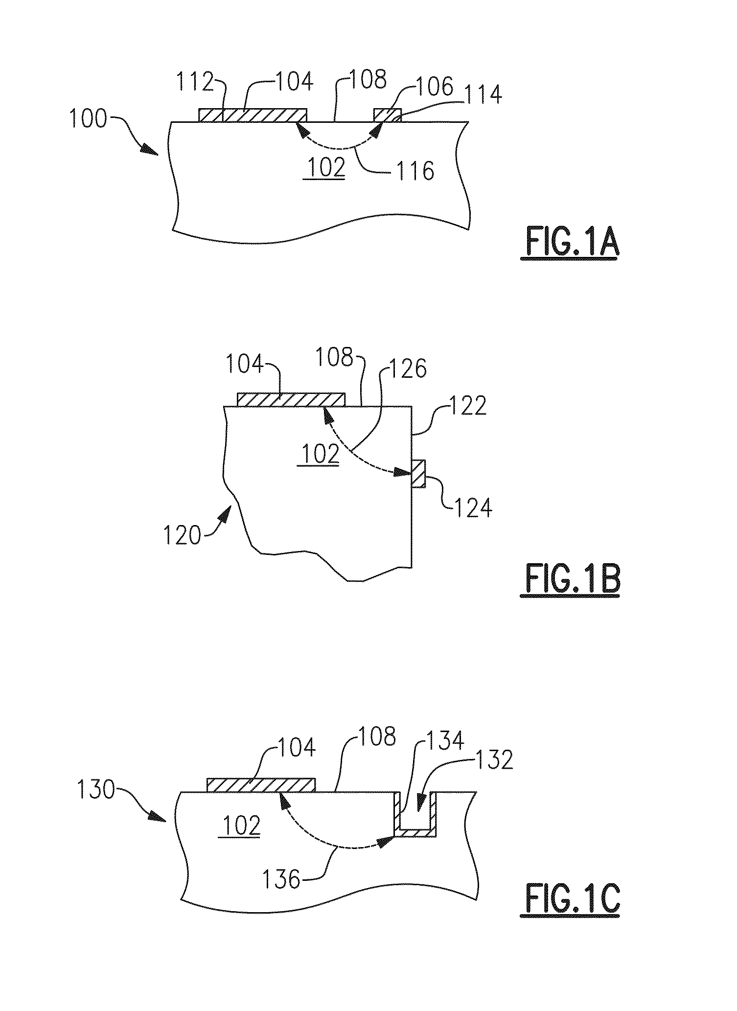
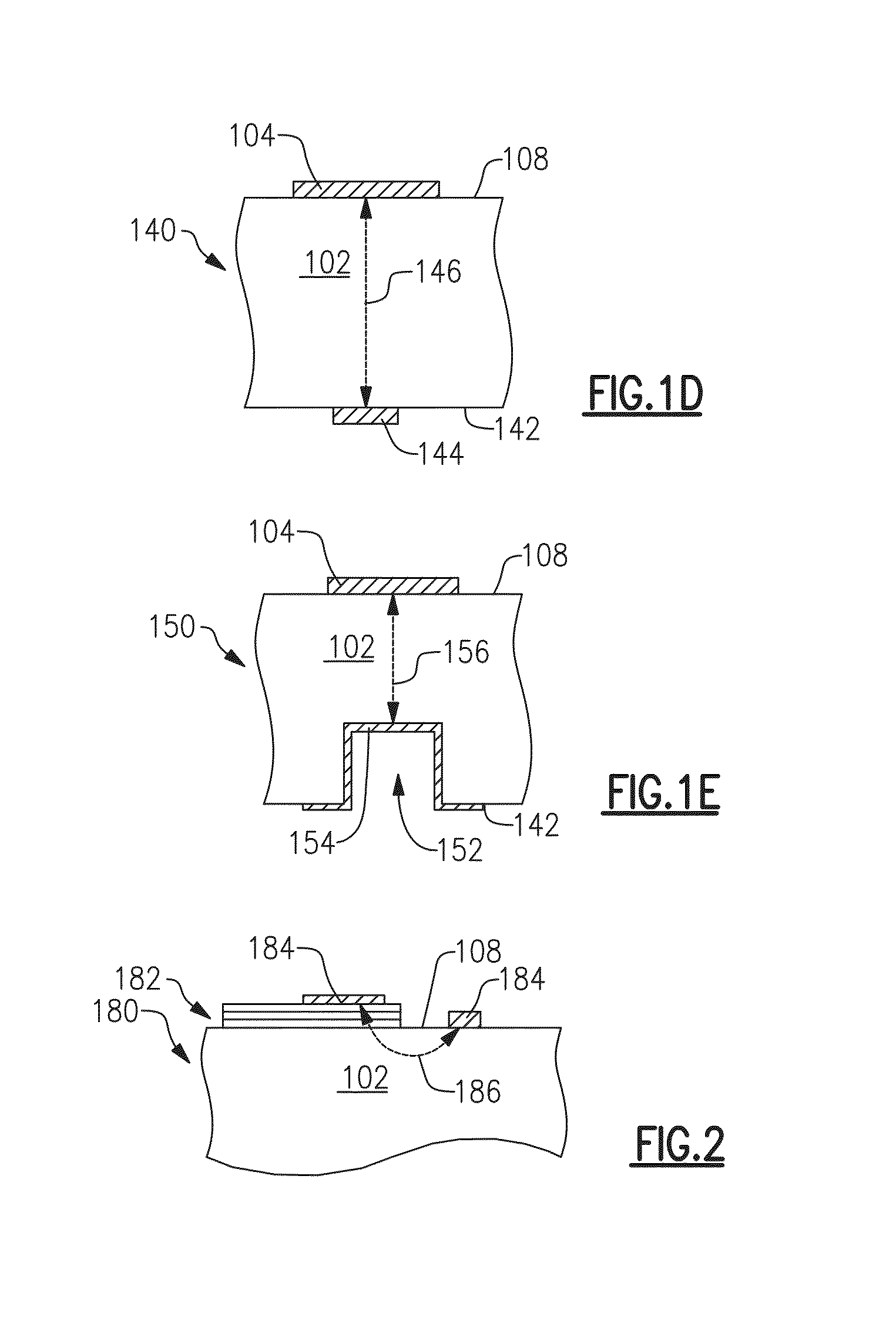
[0063]Described herein are various examples of devices and methods related to an electrostatic discharge (ESD) structure. ESD is generally understood to be a relatively sudden and momentary flow of electrical current between two locations at different electrical potentials.

[0064]In the context of electronics, such unwanted current can damage devices such as integrated circuits (ICs). Such ICs are often formed from semiconductor materials such as silicon and gallium arsenide (GaAs), and such semiconductor materials themselves can suffer damage when subjected to sufficiently high voltages.

[0065]To reduce occurrence of ESDs and / or to mitigate damages resulting from ESDs, antistatic devices and / or ESD protection devices can be provided or formed on IC devices. In some situations, such devices can affect how an IC device operates. For example, a...


PUM


Abstract

Disclosed are systems, devices and methods for utilizing an interconnect conductor to inhibit or reduce the likelihood of de-lamination of a passivation layer of an integrated circuit die. In some implementations, a metal layer in ohmic contact with an intrinsic region of a semiconductor substrate can be partially covered by a passivation layer such as a dielectric layer. An interconnect conductor electrically connected to the metal layer can include an extension that covers an edge of the passivation layer to thereby inhibit the edge from lifting up. In some implementations, the metal layer in combination with a contact pad also in ohmic contact with the intrinsic region can yield a conduction path through the intrinsic region during an electrostatic discharge (ESD) event. In such a configuration, the interconnect conductor can route the ESD charge to a ground.

Description

RELATED APPLICATIONS[0001]This application is a non-provisional of and claims priority to U.S. Provisional Application No. 61 / 588,999, filed on Jan. 20, 2012, entitled “DEVICES AND METHODOLOGIES RELATED TO ELECTROSTATIC DISCHARGE PROTECTION BENIGN TO RF OPERATION,” which is hereby incorporated herein by reference in its entirety.BACKGROUND[0002]1. Field[0003]The present disclosure generally relates to the field of semiconductor technology, and more particularly, to electrostatic discharge protection for semiconductor devices.[0004]2. Description of the Related Art[0005]Electrostatic discharge (ESD) is a sudden and usually undesirable flow of charge between two objects at different electrical potentials. ESD can be harmful to solid state electronics such as integrated circuits.[0006]Some portions of an integrated circuit (IC) can be equipped with ESD protection devices such as diodes. However, such devices typically affect radiofrequency (RF) properties of the IC.SUMMARY[0007]In a nu...

Claims


Application Information

Patent Timeline
IPC IPC(8): H01L23/60H01L23/00
CPCH01L23/60H01L24/03H01L29/872H01L29/66143H01L29/6609H01L29/861H01L2924/1306H01L27/0255H01L2224/05554H01L2924/00H01L23/66H01L24/05H01L25/18H01L27/0292H01L29/868H01L2223/6644H01L2223/6677H01L2223/6683H01L2924/10329H01L2924/12031H01L2924/12032H01L2924/1205H01L2924/1423H01L2924/30205H04B1/16
Inventor SMITH, KIM RENEDICARLO, PAUL T.HILL, MICHAEL DAVID
Owner SKYWORKS SOLUTIONS INC
Why Eureka
Try Eureka