
Optical element for vertical external-cavity surface-emitting laser

a surface-emitting laser and optical element technology, applied in the field of optical elements, can solve the problems of bulky and need sophisticated adjustment, and achieve the effect of increasing the brightness of the vecsel

Inactive Publication Date: 2013-08-29
TRUMPF PHOTONIC COMPONENTS GMBH
View PDF10 Cites 30 Cited by
  • Summary
  • Abstract
  • Description
  • Claims
  • Application Information

AI Technical Summary

Benefits of technology

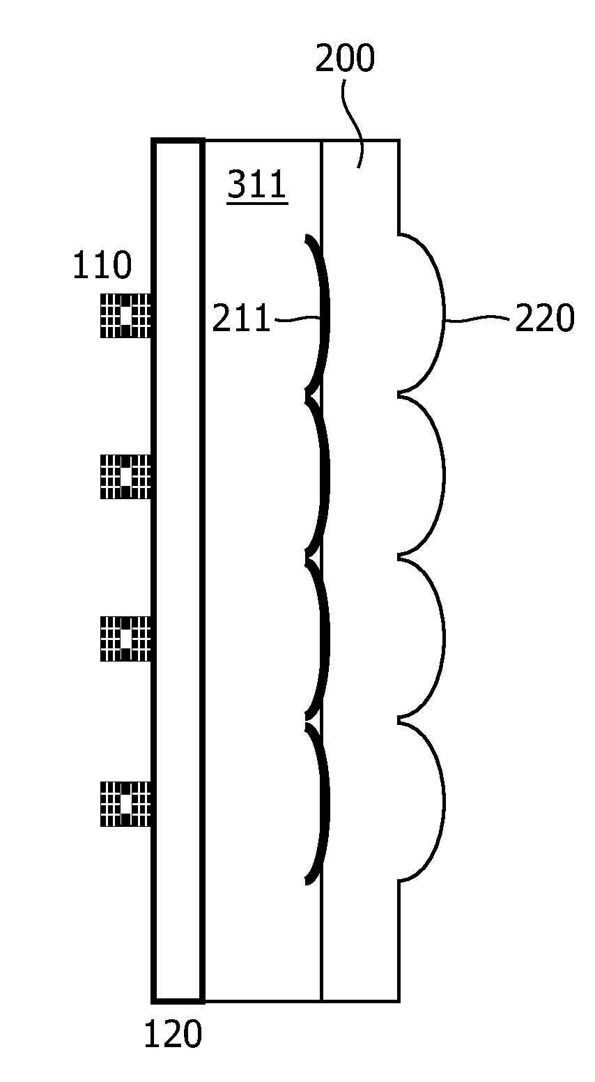
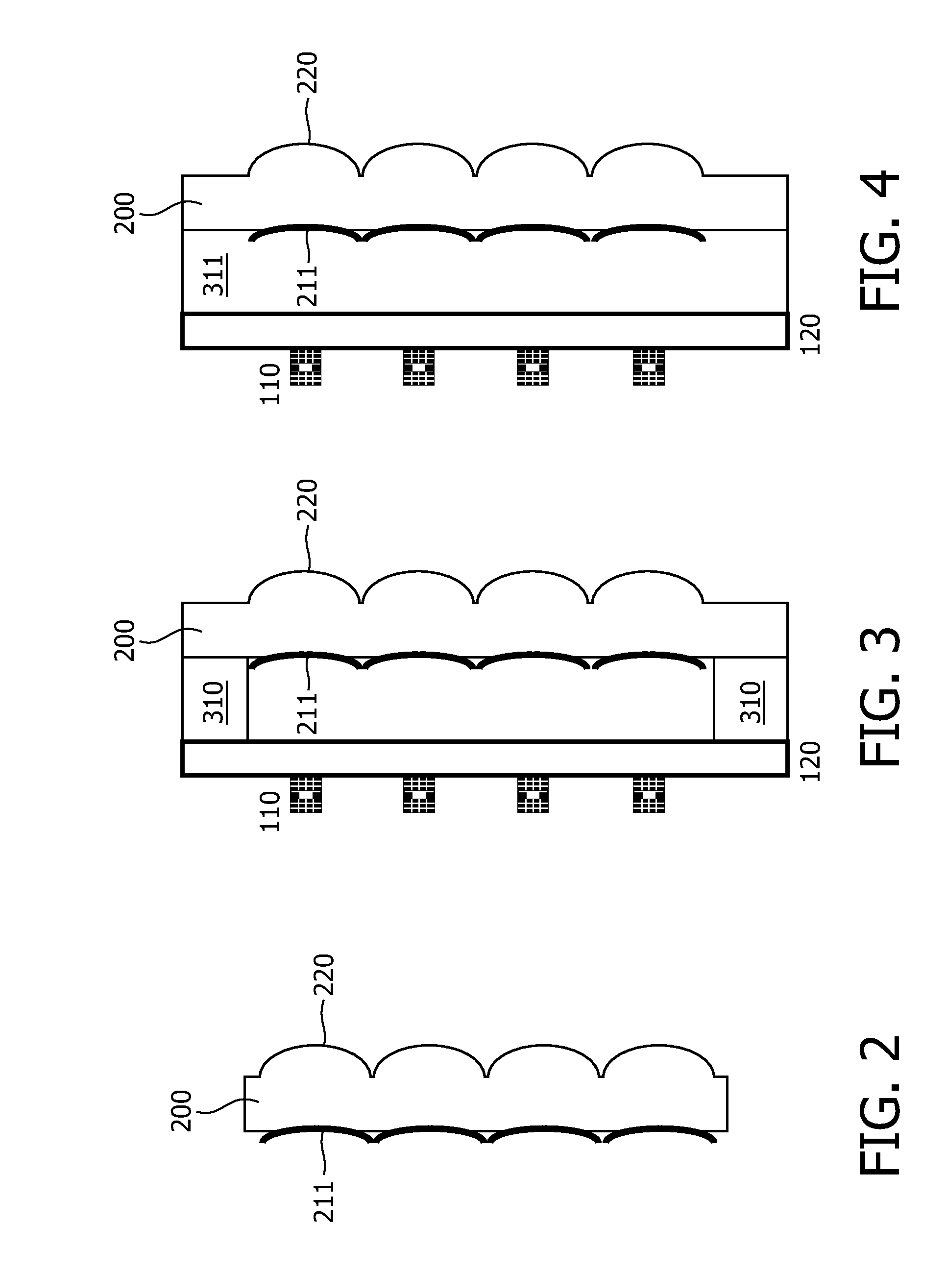
The present invention provides a way to make a VECSEL or VECSEL array brighter without needing to adjust the mirrors during fabrication. This is done by using an optical element that combines the external mirrors of the VECSELs with collimation lenses. The optical element can be fabricated by creating micro-lenses on a glass substrate and applying a reflective coating to them to serve as the external mirrors of the VECSELs. Another layer of micro-lenses with a different radius of curvature is added on top of the first layer to collimate the light coming from the VECSEL. This optical element eliminates the need for additional adjustments to the micro-lenses and simplifies the fabrication process.

Problems solved by technology

In standard setups the external cavity is composed of macroscopic optical elements, which are very bulky and need sophisticated adjustment.

Method used


Image

  • Optical element for vertical external-cavity surface-emitting laser
  • Optical element for vertical external-cavity surface-emitting laser
  • Optical element for vertical external-cavity surface-emitting laser

Examples


Embodiment Construction

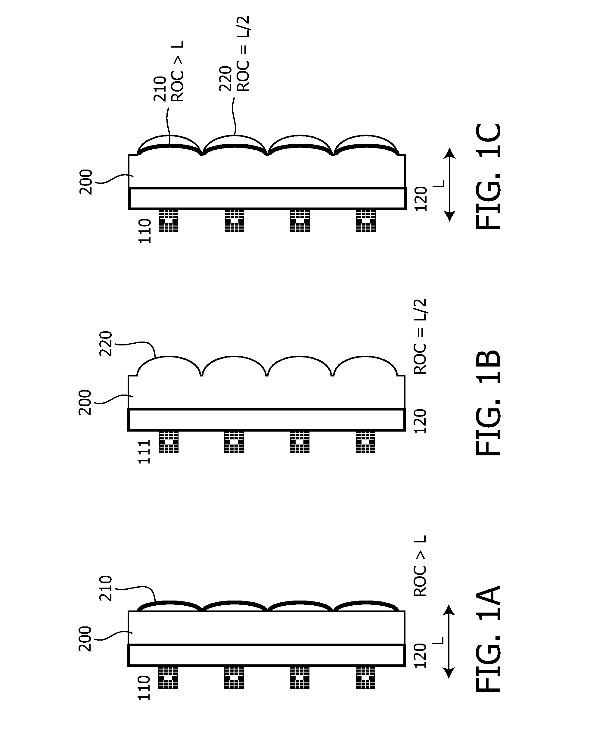
[0019]FIG. 1 shows a comparison of an embodiment of a VECSEL array with the optical element of the present invention compared with solutions of the prior art. FIG. 1A depicts a VECSEL array of the prior art in which the external mirrors are formed on an optically transparent substrate 200 which is attached to the optically transparent carrier substrate 120 on which the semiconductor layer stack 110 of the VECSELs is bonded or grown. This construction is similar to a so called backside or bottom emitting VCSEL which emits the laser radiation through the carrier substrate. The external mirrors on substrate 200 are formed by processing the surface to a spherical (or aspherical) shape (mirror surface 210) and coating a reflective layer on this surface. The radius of curvature (ROC) of the resulting curved regions of the surface fulfill the condition ROC>L, L being the distance of these external concave mirrors to the gain region of the VECSEL.

[0020]In the field of VCSELs it is known to ...


PUM


Abstract

The present invention relates to an optical element for VEC-SELs or VECSEL arrays. The optical element is formed of a substrate (200) which is transparent at least in a wavelength region of optical radiation. A first interface of the- substrate (200) comprises one or several curved regions forming part of an optical lens or of an array of optical lenses (220) integrated in the substrate (200). The substrate (200) further comprises one or several optical mirrors (210) formed on a second interface of the substrate (200) opposing the first interface or embedded in the substrate (200). The optical mirrors (210) are arranged and designed to back reflect a fraction of optical radiation incident on the first or second interface. The optical mirrors (210) are flat mirrors or curved mirrors having a radius of curvature different from the radius of curvature of the curved region (220). The optical element allows the fabrication of a VECSEL or VECSEL array having a high brightness without the requirement of additional adjustments during fabrication. The VECSEL are arranged at a distance (L) to the optical mirrors (210) and this equals the length of the external cavity. The ROC of the optical lens may be chosen to ROC=L / 2 and for the optical mirror ROC>L. The cavity length may be adjusted by a monolithic spacer (120)

Description

FIELD OF THE INVENTION[0001]The present invention relates to an optical element being formed of a substrate, which is transparent at least in a wavelength region of optical radiation, a first interface of said substrate comprising one or several curved regions forming part of an optical lens or of an array of optical lenses integrated in said substrate. The invention also refers to a vertical external-cavity surface-emitting laser (VECSEL) with such an optical element arranged at an emission side of the laser.BACKGROUND OF THE INVENTION[0002]VECSELs are one of the most promising high brightness laser sources and offer many advantages compared to edge emitters, like addressable 2D-array arrangements and circular beam shapes. In standard setups the external cavity is composed of macroscopic optical elements, which are very bulky and need sophisticated adjustment. By realising the external optical components on a wafer and bonding this wafer to the GaAs wafer carrying the semiconductor...

Claims


Application Information

Patent Timeline
Patent Type & Authority Applications(United States)
IPC IPC(8): H01S5/183
CPCG02B19/0057H01S3/08059H01S5/026H01S5/0267H01S5/18361H01S5/18388H01S5/4062H01S5/423H01S5/14
Inventor GRONENBORN, STEPHANMOENCH, HOLGER
Owner TRUMPF PHOTONIC COMPONENTS GMBH
Learn More