Photonic wire bonds

a photonic wire and bonding technology, applied in the field of microoptics and nanooptics, can solve the problems of inability to realize compact photonic wire bonds, inability to create free form curves with variable waveguide cross sections with this method, and strong limitations in the waveguide geometries that can be created with this method

Active Publication Date: 2013-08-29
KARLSRUHER INST FUR TECH
View PDF9 Cites 36 Cited by
  • Summary
  • Abstract
  • Description
  • Claims
  • Application Information

AI Technical Summary

Benefits of technology

[0021]Houbertz, R; Wolter, H.; Dannberg, P; Serbin, J. & Uhlig, S.; “Advanced packaging materials for optical applications: bridging the gap between nm-size structures and large-area panel processing;” Art. No. 612605, Photonics Packaging and Integration VI, 2006, pp. 6126, 12605-12605 discusses inorganic-organic hybrid polymers (so-called ormoceres) with the associated structuring methods based on two-photon polymerization and their uses for the optoelectronics. Discussed as example, among other things, is the production of optical components with two-photon polymerization, wherein it is mentioned as an advantage that these components can be realized on substrates which already contain pre-structured components such as VCSELs or micro-lenses. However, the publication does not discuss the coupling of TPP structured waveguides with integrated optical waveguides. The waveguides described therein are multimodal and thus cannot be coupled without loss to single-mode planar integrated waveguides. The problem defined for the invention therefore cannot be solved with the methods described in this publication.

Problems solved by technology

Free form curves with variable waveguide cross sections cannot be created with this method.
The consequently achievable index contrast is low (typically 0.005), so that realization of compact photonic wire bonds is not possible with this method.
These waveguide structures are oriented per definition on the optical elements to be connected, but the waveguide geometries that can be created with this method are strongly limited.
In particular, it is not possible to generate pre-computed and optimized free-form waveguides.
The use of passive components is furthermore also made more difficult in that these are frequently not transparent for single-photon processes at the lithographic wavelength.
The use of multi-photon polymerization processes in most cases fails because the required capacities frequently cannot be transported in passive structures.
The connection and geometric adaptation of waveguides on pre-positioned optical components is not mentioned and is not feasible with this method since the described imaging method does not permit the three-dimensional position detection.
The structure described therein furthermore has a very low refractive index (estimated at 0.005) which does not allow reaching the high integration density required for photonic wire bonds.
The described waveguides are therefore in principle not suitable for connecting single-mode integrated optical components.
The integration density necessary for photonic wire bonds cannot be achieved with this method.
From this it can be assumed that the spatial resolution that can be achieved with the aforementioned arrangement is in the range of 10 μm, which prevents an efficient optical connection of the generated structures to lateral single-mode, planar integrated waveguides.
The accuracies which can be achieved with this arrangement are limited and, at best, should amount to a few micrometers.
However, the connecting of single-mode connection waveguides to pre-positioned components is not possible with this system for lack of accuracy.
A three-dimensional position detection of components embedded in the resist material is not intended and, accordingly, this arrangement cannot be used to generate waveguide structures which are connected directly and with high precision to planar integrated waveguide-based components.
The measured insertion loss for waveguides produced in this way amounts to 7.8 dB, wherein such high values cannot be tolerated when connecting nano-photonic systems.
The resulting structures, however, have extremely large cross sections and are therefore multimodal and not suitable for solving the object of the present invention.
The waveguides furthermore have a low index contrast and correspondingly large curvature radii and therefore cannot meet the requirements for photonic wire bonds with respect to the integration density.
It can be assumed that the relative position accuracies which can be achieved with this arrangement are not sufficient for connecting single-mode planar integrated waveguides having cross sections of only a few micrometers.
However, the publication does not discuss the coupling of TPP structured waveguides with integrated optical waveguides.
The waveguides described therein are multimodal and thus cannot be coupled without loss to single-mode planar integrated waveguides.

Method used


Image

  • Photonic wire bonds
  • Photonic wire bonds
  • Photonic wire bonds

Examples


Embodiment Construction

[0037]In the drawings, like reference numbers are used to denote like components in the different figures.

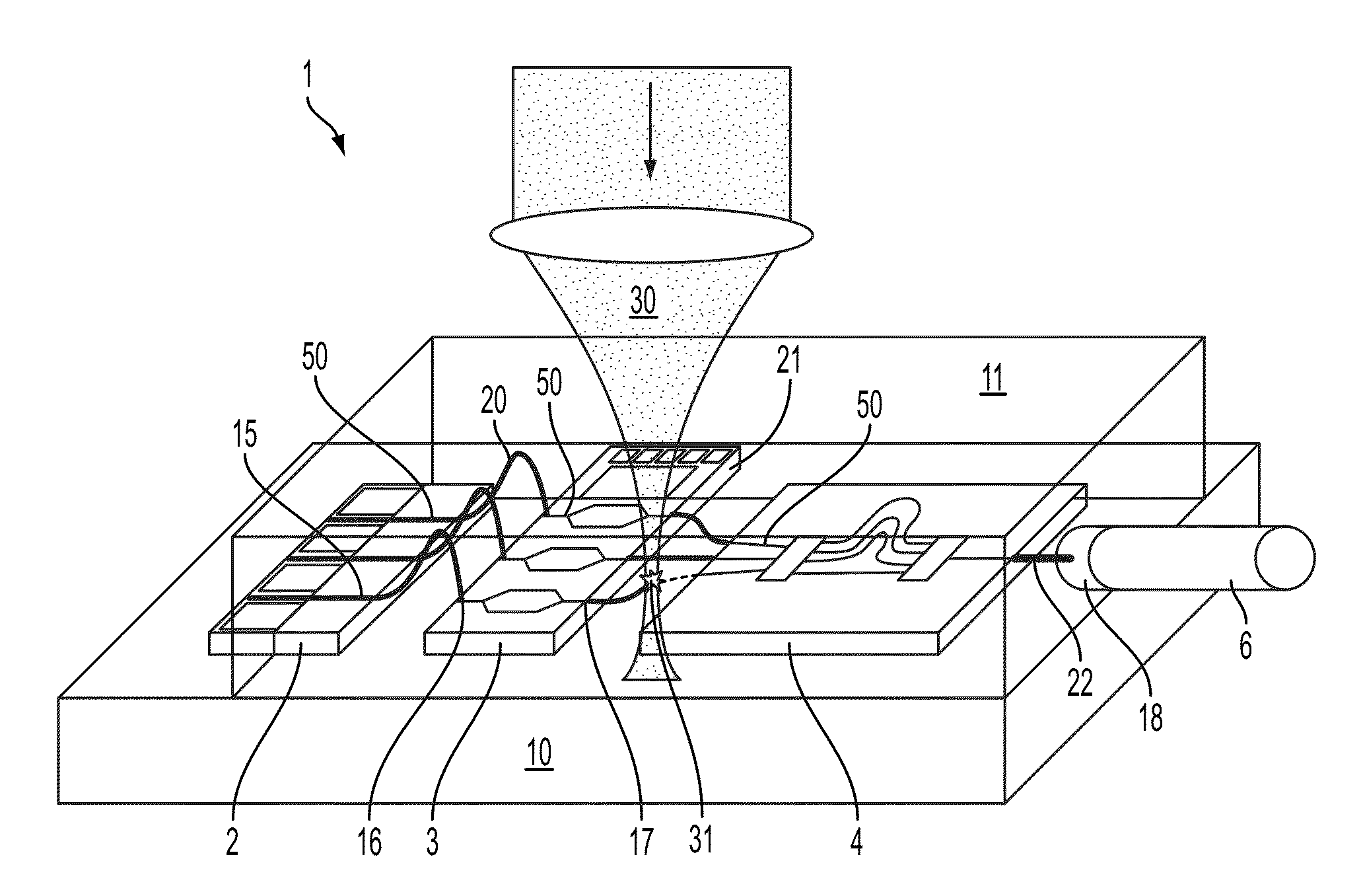
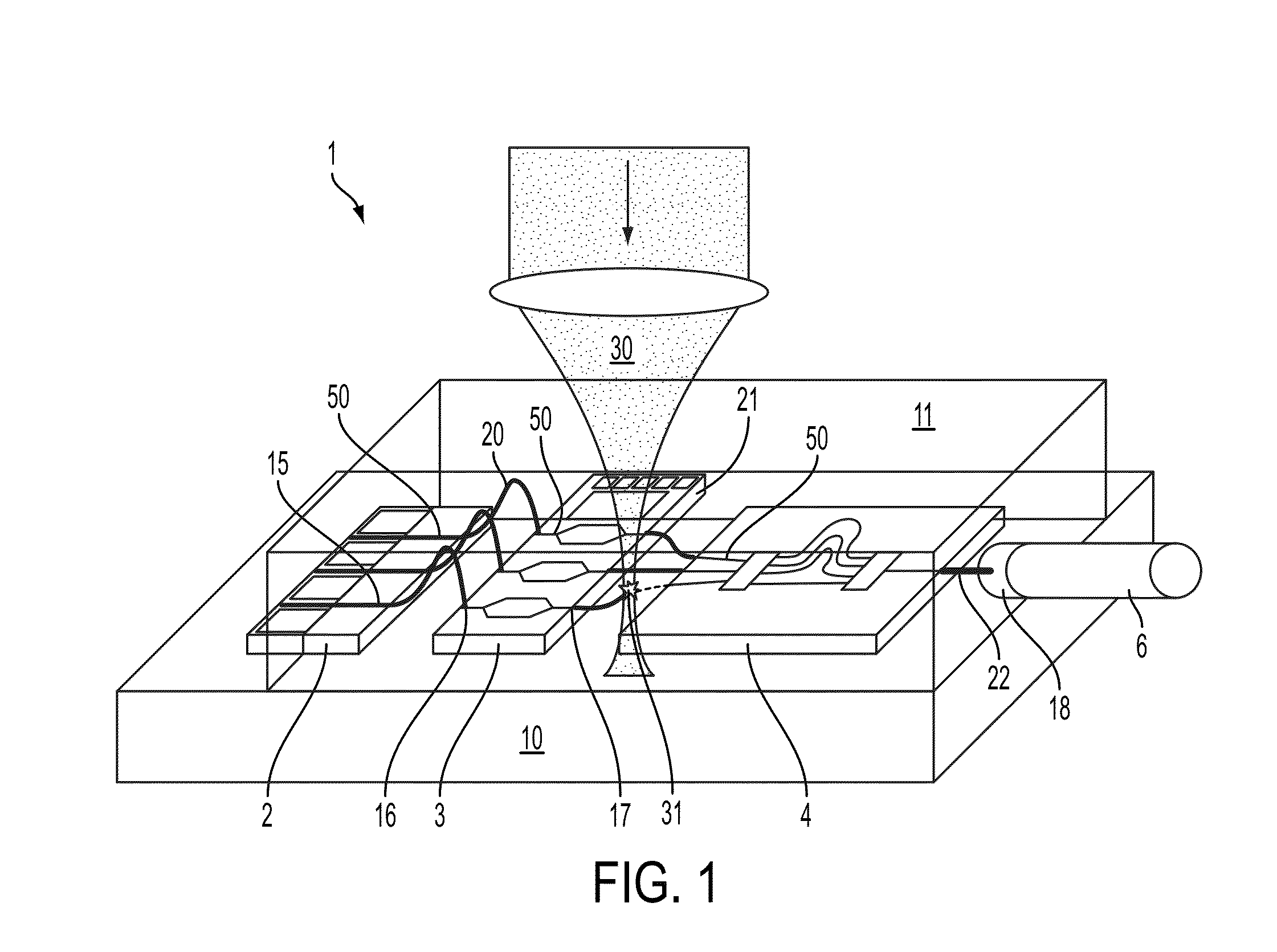
[0038]The waveguide structures upon which the invention is based are intended for the low-loss optical connection of lateral single-mode planar integrated photonic systems. The functional principle of the invention is explained with the example of the arrangement illustrated in FIG. 1. The optical arrangement (1) consists of several photonic systems that are planar integrated on different substrates (2-4) (“chips”) and which contain lateral single-mode waveguides (50). The waveguides (50) positioned on different chips are to be interconnected and / or are to be connected to output and input waveguides (5-6) (see also FIGS. 12-15), only input / output waveguide (6) being shown in FIG. 1. For this, the elements (2-6) to be connected are mounted on a component carrier (10) and are covered at least partially with a resist material (11). Each of the elements to be connected comprises opt...


PUM


Abstract

An optical arrangement includes a plurality of planar substrates with at least one planar integrated optical waveguide on each planar substrate. At least one optical waveguide structure has at least one end connected via an optical connecting structure to one of the planar integrated optical waveguides. The optical waveguide structure is positioned at least partly outside the integration plane for the planar integrated optical waveguide and a refractive index contrast between a core region and a cladding region of the optical waveguide structure is at least 0.01.

Description

BACKGROUND[0001]1. Technical Field[0002]The invention relates to the field of micro-optics and nano-optics, and more particularly relates to waveguide structures for optical interconnection of planar-integrated photonic systems (chip-chip connections) and the connection of planar integrated photonic systems to glass fibers (fiber-chip connection). The invention furthermore relates to a method and a device for producing the waveguide structures.[0003]The field of integrated optics, in particular the area of silicon photonics, meaning the integration of waveguide-based photonic components on silicon or silicon-on-insulator (SOI) substrates, has been the subject of intensive research and development work for several years. This technology permits transferring mature CMOS (complementary metal oxide semiconductor) processes, developed for mass production of integrated electronic circuits, to the integrated photonic. Nano-photonic systems with high complexity and a plurality of functional...

Claims


Application Information

Patent Timeline
Patent Type & Authority Applications(United States)
IPC IPC(8): G02B6/12
CPCG02B6/30G02B6/138G02B6/43
Inventor KOOS, CHRISTIANFREUDE, WOLFGANGLINDENMANN, NICOLELEUTHOLD, JUERG
Owner KARLSRUHER INST FUR TECH
Why Eureka
Try Eureka