

Algorithm of cu interconnect dummy inserting
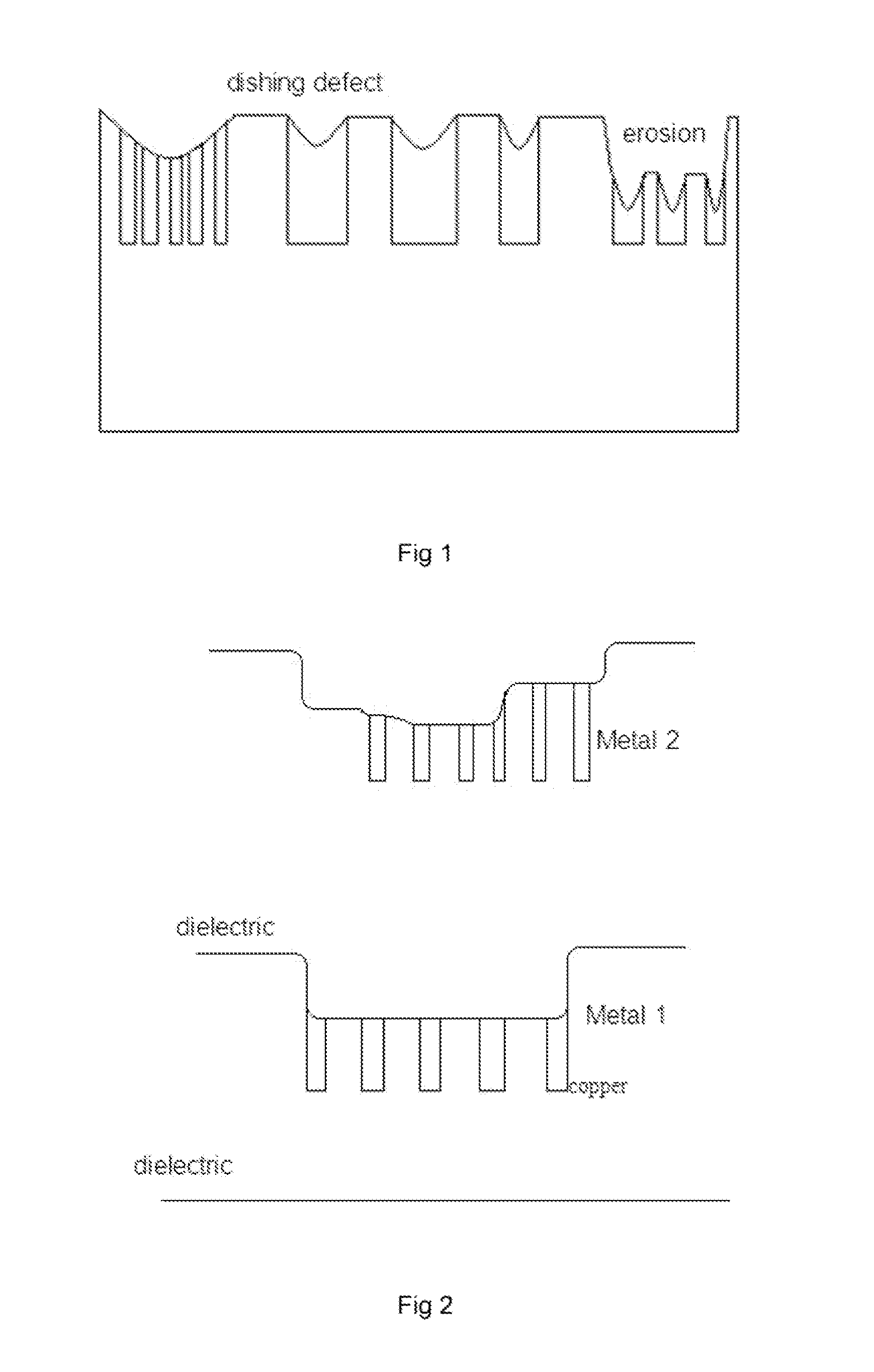
a technology of interconnect dummy and algorithm, which is applied in the field of algorithm of interconnect dummy inserting, can solve the problems of strong correlation between dishing defect and insurmountable technology and integration difficulties, affecting the yield and reliability of the product, and the effect of insufficient integration
- Summary
- Abstract
- Description
- Claims
- Application Information
AI Technical Summary
Benefits of technology
Problems solved by technology
Method used
Image

Examples
Embodiment Construction
[0041]The following context will make further description for the present invention in conjunction with appended drawings and specific embodiments, but not act as a limitation for the present invention.
[0042]An algorithm of Cu interconnect dummy inserting, comprising semiconductor chip on a substrate, semiconductor chip including signal trace, signal trace is mainly formed by patterning metal layer.
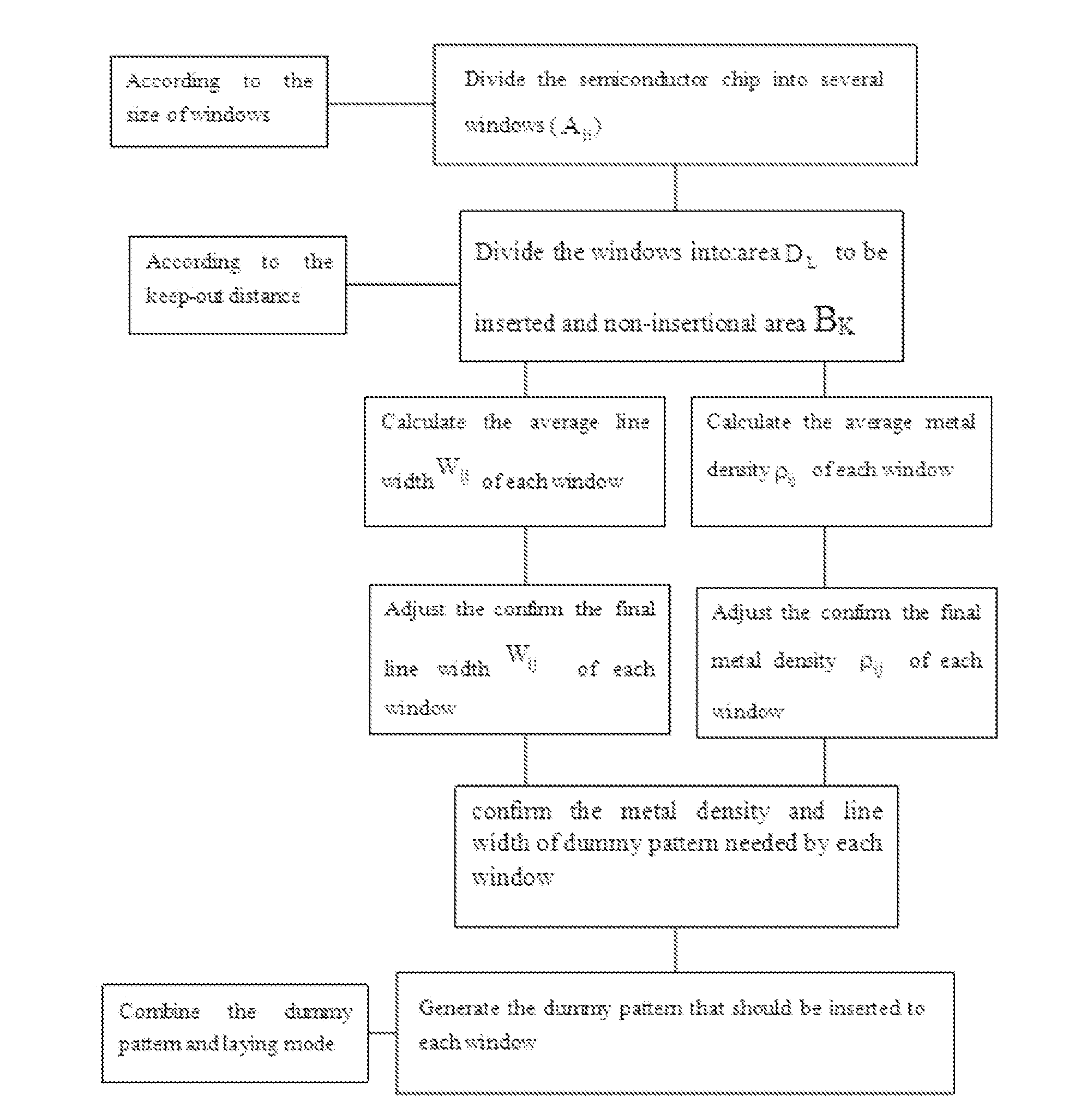
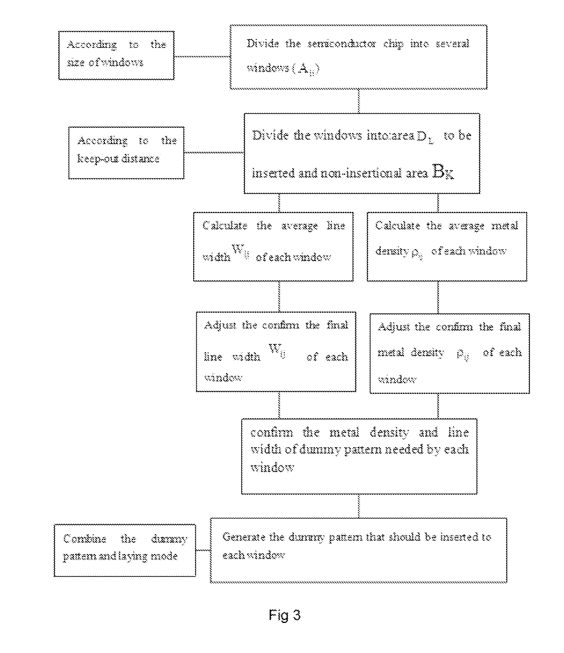
[0043]Illustrated as FIG. 3, the process of the inserting algorithm comprises the following steps:
[0044]Step 1, divide the surface of semiconductor chip into several square windows with an area of A illustrated as FIG. 4, each of which is non-overlapping. Each window is indicated by Aij (the sum of Aij is m*n);
[0045]Step 2, Perform a logic operation on each square window and the window is divided into two parts shown in FIG. 5: the area to-be-inserted which need dummy pattern filling and it is indicated by DL, L is any number from 1 to m the non-inserting area which needn't dummy pattern ...
PUM
 Abstract
Description
Claims
Application Information