Substrate structure and fabrication method thereof

Inactive Publication Date: 2013-09-05
SILICONWARE PRECISION IND CO LTD
View PDF2 Cites 2 Cited by
  • Summary
  • Abstract
  • Description
  • Claims
  • Application Information

AI Technical Summary

Benefits of technology

[0019]According to the present invention, each of the conductive pads merely contains little copper besides nickel and gold such that the bonding layer between the conductive pad and the corresponding solder balls is mainly comprised of Cu6Sn5 ins

Problems solved by technology

Therefore, during a drop test, the solder ball may easily fall off from the conductive pad.
Therefore, during a drop test, the solder ball is not easy to fall off.
However, compared with the gold layer 13, the OSP

Method used


Image

  • Substrate structure and fabrication method thereof
  • Substrate structure and fabrication method thereof
  • Substrate structure and fabrication method thereof

Examples


first embodiment

[0026]FIGS. 3A to 3E are schematic cross-sectional views showing a substrate structure and a fabrication method thereof according to a first embodiment of the present invention.

[0027]Referring to FIG. 3A, a substrate body 30 is provided and a plurality of conductive pads 31 (only one conductive pad is illustrated in the drawing) are formed on the substrate body 30. Each of the conductive pads 31 has a first copper layer 311 and a nickel layer 312 formed on the first copper layer 311.

[0028]Referring to FIG. 3B, a second copper layer 313 and a gold layer 314 are sequentially formed on the nickel layer 312. The second copper layer 313 has a thickness less than that of the first copper layer 311.

[0029]Referring to FIG. 3C, a solder flux 32 is formed on the gold layer 314 so as for a solder ball 33 to be mounted thereon.

[0030]Referring to FIG. 3D, a reflow process is performed so as to volatilize the solder flux 32 and dissolve the gold layer 314 into the solder ball 33 and also dissolve...

second embodiment

[0036]FIGS. 4A to 4D are schematic cross-sectional views showing a substrate structure and a fabrication method thereof according to a second embodiment of the present invention.

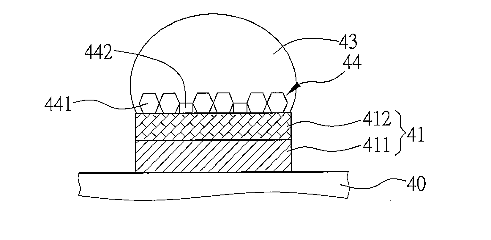
[0037]Referring to FIG. 4A, a substrate body 40 is provided and a plurality of conductive pads 41 are formed on the substrate body 40. Each of the conductive pads 41 has a copper layer 411.

[0038]Referring to FIG. 4B, a nickel-copper mixed layer 412 and a gold layer 413 are sequentially formed on the copper layer 411. In the nickel-copper mixed layer 412, the content of copper is less than the content of nickel.

[0039]Referring to FIG. 4C, a solder flux 42 is formed on the gold layer 413 so as for a plurality of solder balls 43 to be mounted thereon. Referring to FIG. 4D, a reflow process is performed to volatilize the solder flux 42 and dissolve the gold layer 413 into the solder ball 43, thus forming a bonding layer 44 between the solder ball 43 and the nickel-copper mixed layer 412. The bonding layer 44 is ...


PUM


Abstract

A substrate structure includes a substrate body and a plurality of conductive pads formed on the substrate body and each having a first copper layer, a nickel layer, a second copper layer and a gold layer sequentially stacked. The thickness of the second copper layer is less than the thickness of the first copper layer. As such, the invention effectively enhances the bonding strength between the conductive pads and solder balls to be mounted later on the conductive pads, and prolongs the duration period of the substrate structure.

Description

BACKGROUND OF THE INVENTION[0001]1. Field of the Invention[0002]The present invention relates to substrate structures and fabrication methods thereof, and more particularly, to a substrate structure having solder balls for external electrical connection and a fabrication method thereof.[0003]2. Description of Related Art[0004]Ball grid array (BGA) semiconductor package structures have been developed to meet the trend of lighter, thinner, shorter and smaller electronic products. In such a BGA semiconductor package structure, a semiconductor chip is disposed on a surface of a substrate and electrically connected to the substrate through a plurality of bonding wires, and a plurality of solder balls are mounted on conductive pads of the other surface of the substrate, respectively, so as to electrically connect another electronic device such as a circuit board or another package structure.[0005]FIGS. 1A and 1B are schematic cross-sectional views of a conductive pad in a conventional sub...

Claims


Application Information

Patent Timeline
IPC IPC(8): H01L23/485H01L21/768H01L21/60H01L23/488
CPCH01L23/3128H01L24/32H01L23/49816H01L23/49811H01L2224/48227H05K3/3478H05K3/3436H05K3/244H01L2224/73265H01L24/48H01L2224/32225H01L2224/48091H01L2224/48105H01L2924/00014H01L2924/00H01L2924/181H01L2924/00012H01L2224/45099H01L2224/45015H01L2924/207
Inventor HUNG, LIANG-YIPAI, YU-CHENGHSIAO, WEI-CHUNGLIN, CHUN-HSIENSUN, MING-CHEN
Owner SILICONWARE PRECISION IND CO LTD
Why Eureka
Try Eureka