

Semiconductor apparatus and method for producing the same
a semiconductor and apparatus technology, applied in the direction of semiconductor devices, semiconductor/solid-state device details, electrical apparatus, etc., can solve the problems of deterioration of disable the production of semiconductor apparatuses, etc., and achieve less residual strain, and excellent heat resistance and moisture resistance.
- Summary
- Abstract
- Description
- Claims
- Application Information
AI Technical Summary
Benefits of technology
Problems solved by technology
Method used
Image

Examples
example 1
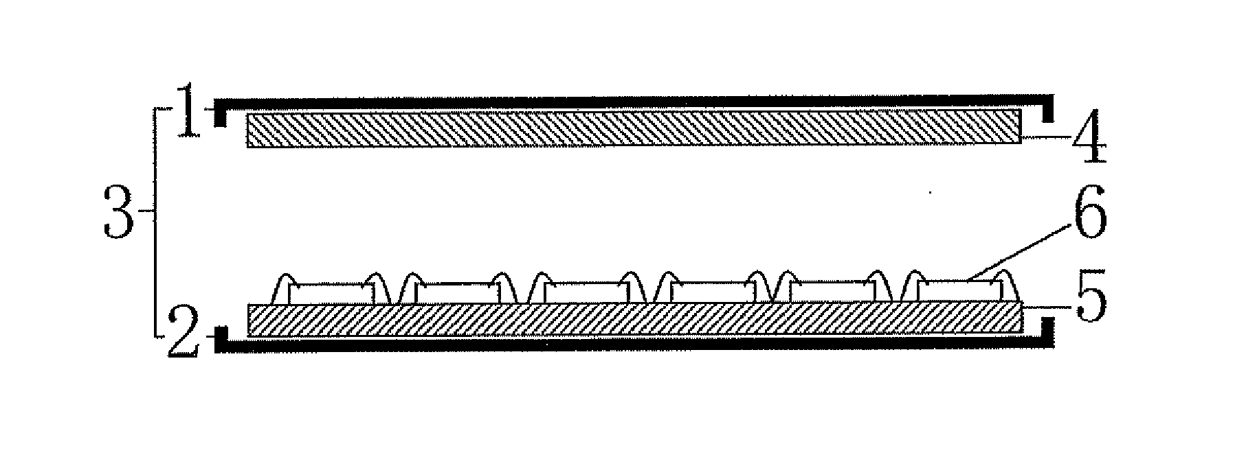
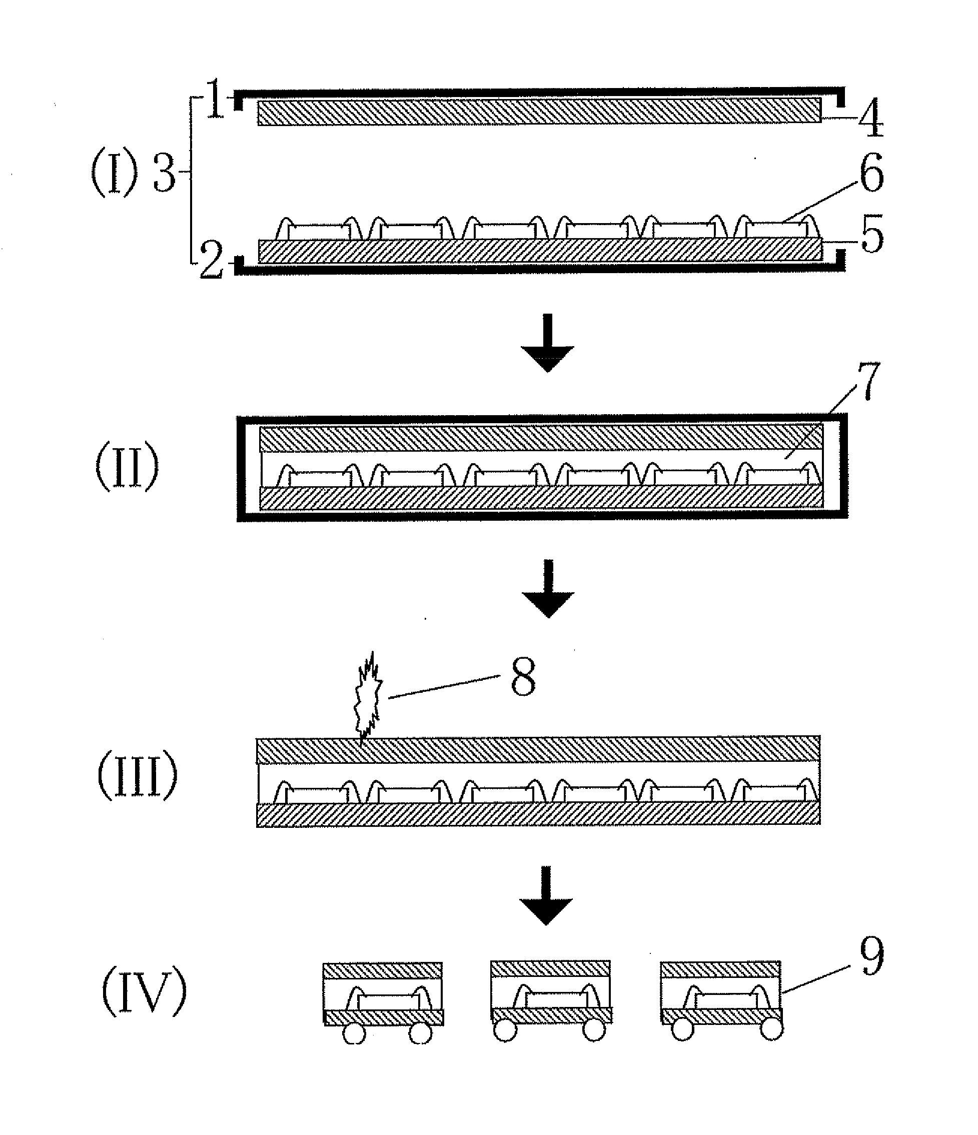
[0073]The following organic resin substrate on which semiconductor devices were mounted and organic resin substrate on which no semiconductor devices was mounted were prepared:
[0074]Organic resin substrate on which semiconductor devices were mounted of BT resin substrate (linear expansion coefficient of 15 ppm / ° C.) of 50 μm thickness, 50 mm width, and 150 mm length, having 40 silicon chips each being 12 mm square and having 300 μm thickness, bonded to the substrate by an epoxy die bonding material, where the substrate and chips were connected by gold wires; and
[0075]Organic resin substrate on which no semiconductor device was mounted of BT resin substrate (linear expansion coefficient of 15 ppm / ° C.) of 50 μm thickness, 50 mm width, and 150 mm length.
[0076]In a transfer molding machine, a mold temperature was set at 170° C., and the organic resin substrate on which semiconductor devices were mounted was attached by suction onto a lower mold half of the mold. In turn, the organic re...
example 2
[0080]Prepared were the same organic resin substrate on which semiconductor devices were mounted and the same organic resin substrate on which no semiconductor device was mounted, as those used in Example 1. In a compression molding machine, a mold temperature was set at 170° C., and the organic resin substrate on which semiconductor devices were mounted was attached by suction onto a lower mold half of the mold. In turn, the organic resin substrate on which no semiconductor device was mounted was attached by suction onto an upper mold half of the mold in the same manner. A predetermined amount of thermosetting epoxy resin in a liquid state was then put onto a central portion of the substrate arranged by suction on the lower mold half, then the epoxy resin was pressurized by the upper and lower mold halves at 100 Kg / cm2 and cured until the thickness of the resin was brought to 500 μm.
[0081]After molding, the integrated substrates were taken out of the mold, and cooled down to a room...
example 3
[0083]The following silicon wafers were prepared:
[0084]Silicon wafer formed with semiconductor devices thereon of silicon wafer having a thickness of 350 μm and a diameter of 8 inches (200 mm), and formed with semiconductor devices thereon; and
[0085]Silicon wafer formed with no semiconductor devices thereon: silicon wafer having a thickness of 350 μm and a diameter of 8 inches (200 mm), and formed with no semiconductor devices thereon.
[0086]In a compression molding machine, a mold temperature was set at 170° C., and the silicon wafer formed with semiconductor devices was attached by suction onto a lower mold half of the mold. In turn, the silicon wafer formed with no semiconductor device was attached by suction onto an upper mold half of the mold in the same manner as the wafer formed with semiconductor devices, a predetermined amount of thermosetting epoxy resin (SMC800 produced by Shin-Etsu Chemical Co., Ltd.) in a liquid state was then put on a central portion of the wafer arrang...
PUM
| Property | Measurement | Unit |
|---|---|---|
| temperature | aaaaa | aaaaa |
| diameter | aaaaa | aaaaa |
| thickness | aaaaa | aaaaa |
Abstract
Description
Claims
Application Information