Conductive pattern film substrate and manufacturing method

a technology of conductive pattern and substrate, which is applied in the direction of 3d rigid printed circuits, metal pattern materials, railway signalling, etc., can solve the problems of low conforming rate of finished products, complex process, and high cos

Inactive Publication Date: 2013-09-26
CHANG JACKY +6
View PDF1 Cites 3 Cited by
  • Summary
  • Abstract
  • Description
  • Claims
  • Application Information

AI Technical Summary

Benefits of technology

[0009]Yet another objective of the present invention is to provide the aforesaid manufacturing method and the substrate for melting and transforming a metal (such as zinc, copper, silver, stainless steel, aluminum, gold, or the like) into tiny metal particles (also known as minute particles) instantaneously by a thermal spraying source, spraying directly the tiny metal particles to a body (made of a material, such as plastic, plastic film, ceramic, metal, or glass) having a pattern layer, forming a metal-containing film layer on the body by particle stacking, thereby enabling the multi-dimension pattern layer (such as an antenna pattern, an electrical circuit pattern, or any other appropriate pattern) to acquire the electrical characteristics intended by the pattern.

Problems solved by technology

However, the aforesaid laser-shaping manufacturing process has drawbacks, such as high costs, an intricate process, a low conforming rate of a finished product, and an environmentally unfriendly electroplating process.
Although the aforesaid technique dispenses with a dedicated plastic material, the use of a conductive paint has its own disadvantages.
For example, the manufacturing process requires a large amount of solvent, filler, and additive, such as polymer resin.
The additive is likely to bind with conductive metal particles to thereby produce a large amount of volatile organic compounds (VOC) waste gas pollution and thus compromise environmental protection.

Method used


Image

  • Conductive pattern film substrate and manufacturing method
  • Conductive pattern film substrate and manufacturing method
  • Conductive pattern film substrate and manufacturing method

Examples


first embodiment

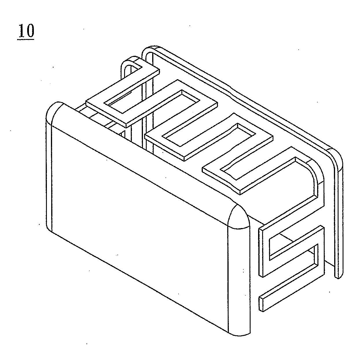
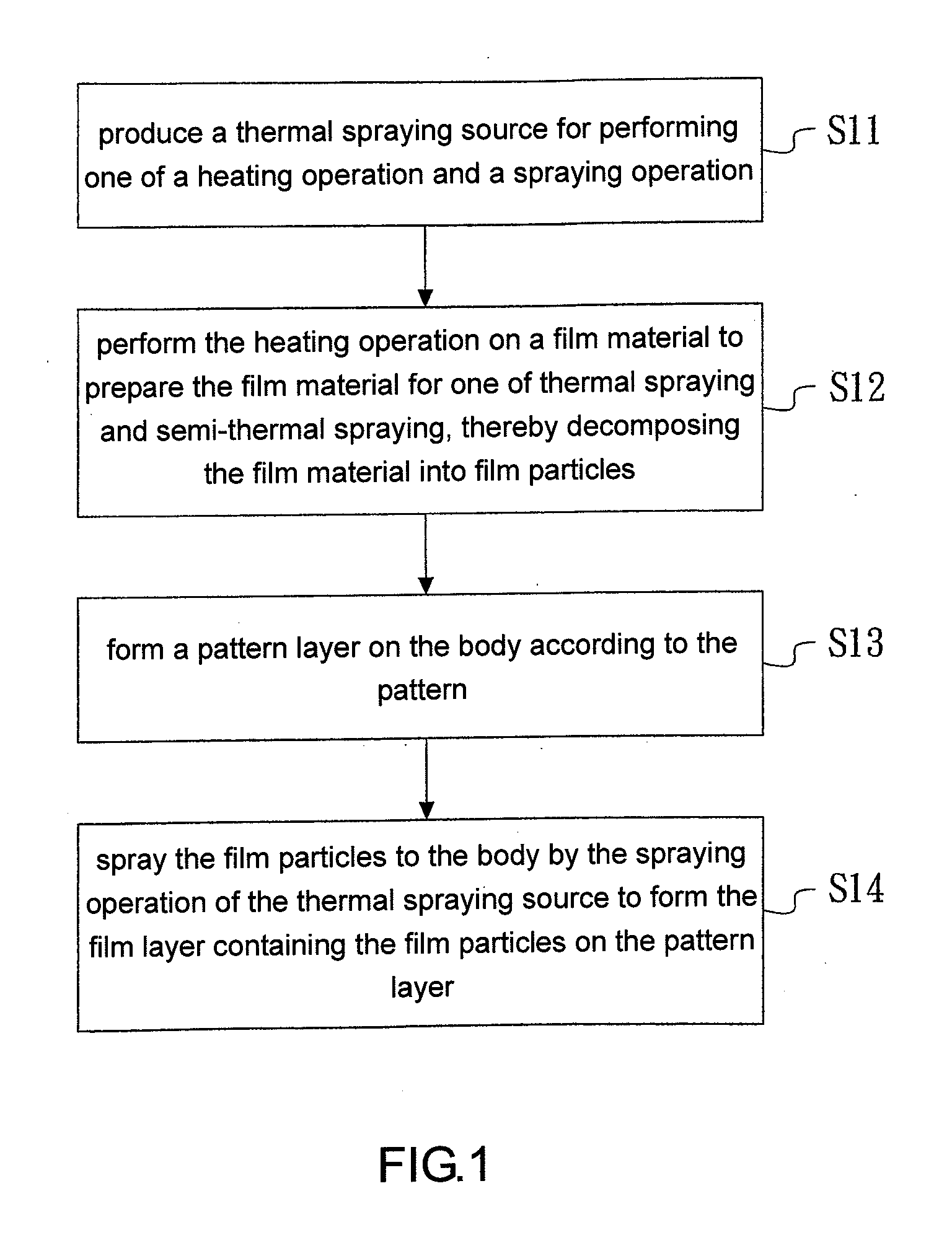
[0019]Referring to FIG. 1, there is shown a flow chart of a conductive pattern film substrate manufacturing method according to the present invention. As shown in FIG. 1, the conductive pattern film substrate manufacturing method for combining two anisotropic materials, namely a patterned body and a film layer, without assistance from an intermediate layer. The body comes in the form of a sticker, a tablet PC casing, a notebook computer casing, a handheld electronic device casing, or a casing for any other electronic device.

[0020]The process flow of the conductive pattern film substrate manufacturing method starts from step S11 that involves producing a thermal spraying source for performing a heating operation or a spraying operation. In this step, depending on the form of energy, the thermal spraying source is of two types, namely a thermal source and an electrical source. For example, thermal spraying source can be produced by combustion flame spraying, powder flame spraying, wir...

second embodiment

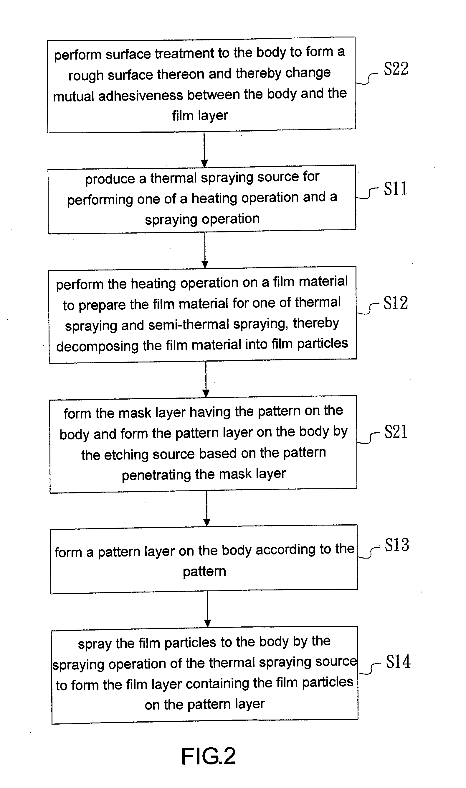
[0027]Referring to FIG. 2, there is shown a flow chart of the conductive pattern film substrate manufacturing method according to the present invention. As shown in FIG. 2, in addition to the aforesaid steps S11˜S14, the conductive pattern film substrate manufacturing method further comprises step S21 that entails forming the mask layer having the pattern on the body and forming the pattern layer on the body by the etching source based on the pattern penetrating the mask layer. This step applies to two embodiments. In one of the two applicable embodiments, a hole corresponding in position to the pattern is formed in the mask layer or the mask casing, and the body is covered with the mask layer, such that the etching source performs etching on the body through the hole, so as to form the pattern layer on the body. In the other applicable embodiment, the body is covered with the mask layer (or the mask casing), and the required pattern or an additional pattern is drawn on the mask lay...


PUM

PropertyMeasurementUnit
conductiveaaaaaaaaaa
adhesivenessaaaaaaaaaa
electrical characteristicsaaaaaaaaaa

Abstract

A conductive pattern film substrate and manufacturing method for combining two anisotropic materials, namely a patterned body and a film layer, without assistance from an intermediate layer. The method includes producing a thermal spraying source for performing a heating operation on a film material to prepare the film material for thermal spraying or semi-thermal spraying and thereby decompose the film material into film particles; and spraying the film particles to a pattern layer disposed on the body and having the pattern by the thermal spraying source to form the film layer having the film particle on the pattern layer, thereby enabling the body to embody electrical characteristics of the pattern.

Description

FIELD OF THE INVENTION[0001]The present invention relates to conductive pattern film substrates and manufacturing methods, and more particularly, to a substrate for forming a conductive pattern film on a body (comprising ceramic, plastic, polymeric plastic, glass, metal, or the like, for example) and a method thereof.BACKGROUND OF THE INVENTION[0002]According to related prior art, a 3-dimension circuit is applicable to a casing of an electronic device, and a circuit layout of a printed circuit board (PCB) is formed on the casing by laser technology and electroplating technology. For example, an antenna is formed on the casing by laser direct structuring (LDS).[0003]However, the aforesaid laser-shaping manufacturing process has drawbacks, such as high costs, an intricate process, a low conforming rate of a finished product, and an environmentally unfriendly electroplating process. For example, the laser-shaping technology entails performing laser etching with an expensive dedicated p...

Claims


Application Information

Patent Timeline
Patent Type & Authority Applications(United States)
IPC IPC(8): H05K1/09H05K3/22B24C1/00B05D3/06H05K1/00B26D3/08H05K3/00B29C71/04
CPCB24C3/322B29C59/00B29C59/10B29C59/16B29C2059/027B29C2791/009H05K2203/0548H05K3/14H05K3/381H05K2201/09263H05K2201/10098H05K2203/1344H05K1/0284Y10T83/0341
Inventor CHANG, JACKYLIN, ERICLIU, SONG-JHE
Owner CHANG JACKY
Why Eureka
Try Eureka