Plasma resistant member, manufacturing method for the same and method of forming a thermal spray coat

a technology of plasma resistant and protective layer, which is applied in the direction of plasma technique, coating, natural mineral layered products, etc., can solve the problems of insufficient anchoring effect, defective products at the semiconductor production process, and high cost of plasma resistant ceramics, so as to prevent the occurrence of microcracks, prevent the exfoliation of plasma resistant protective layer, and high adhesion strength

Inactive Publication Date: 2006-02-23
COVALENT MATERIALS CORP
View PDF6 Cites 49 Cited by
  • Summary
  • Abstract
  • Description
  • Claims
  • Application Information

AI Technical Summary

Benefits of technology

[0011] The present invention has been worked out under these circumstances. An object of the present invention is to provide a plasma resistant member having a plasma resistant coating layer with high adhesion strength on the surface thereof and a manufacturing method for the same. Another object of the present invention is to provide a method for forming a protective layer and a manufacturing method for a composite material, both of methods are capable of preventing an occurrence of microcracks on the surface of the ceramic material and also preventing the exfoliation of plasma resistant protective layer, when forming a protective layer having a plasma resistant layer on a brittle material such as a ceramic by a thermal spray.

Problems solved by technology

These plasma resistant ceramics are expensive and thus reduction of cost is desired.
Accordingly, when the adhesion strength between these materials is poor, the plasma resistant surface layer can be exfoliated from the alumina base material during the use of the plasma resistant member, causing the occurrence of defective products at the semiconductor production process.
However, the aforementioned roughening method involving sandblasting cannot provide a sufficient anchoring effect.
Therefore, there are some problems of spray coat exfoliation.
Accordingly, the resulting anchoring effect, if any, is insufficient.
Therefore, the sandblasting method is disadvantageous in that the surface of the ceramic member itself can cause contamination by particles.
Further, because the formation of the roughened surface on the ceramic material is accompanied by the occurrence of microcracks on the surface of the ceramic material, when thermal spray coat is formed on the ceramic material having these microcracks, a sufficient anchoring effect cannot be exerted.
Some materials having a remarkably high strength, such as quartz, have a possibility of breaking the base material due to the microcracks.
Accordingly, when the adhesion strength between the base material and the thermal spray coat is too small, the thermal spray coat can be exfoliated and thus cannot act as a protective layer.
Further, serious problems such as generation of particles can arise.

Method used


Image

  • Plasma resistant member, manufacturing method for the same and method of forming a thermal spray coat
  • Plasma resistant member, manufacturing method for the same and method of forming a thermal spray coat
  • Plasma resistant member, manufacturing method for the same and method of forming a thermal spray coat

Examples


first embodiment

(Plasma Resistant Member)

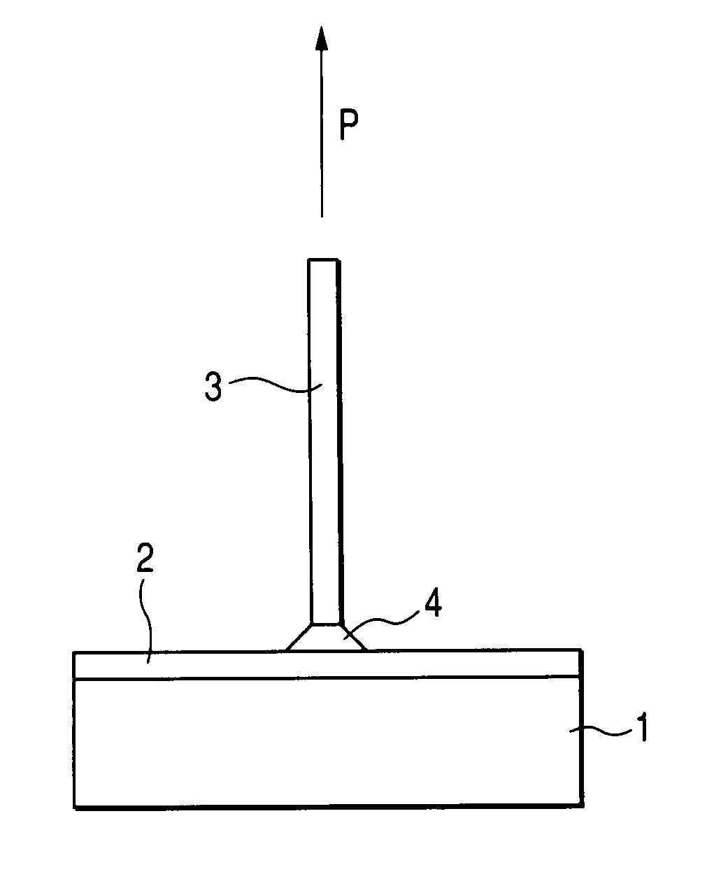
[0054] A first embodiment of implementation of the present invention will be described hereinafter. In the plasma resistant member according to the present embodiment, the surface roughness Ra of the alumina base material is ranging from 5 μm to 15 μm, and a surface layer made of Y2O3 or YAG is formed on the roughened surface of the alumina base material, whereby the plasma resistance thereof can be improved. In the present embodiment of implementation of the present invention, the surface roughness Ra of the alumina base material falls within the above defined range, making it possible to predetermine the adhesion strength between the surface of the alumina base material and the surface layer of the plasma resistant member to 8 MPa or more. Whenever the surface roughness Ra of the alumina base material falls outside the above defined range, the adhesion strength between the surface of the alumina base material and the surface layer of the plasma resistant...

second embodiment

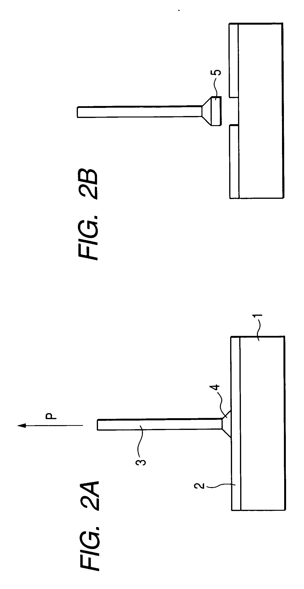
[0070] While the first embodiment has been described with reference to the case where the surface of an alumina base material is subjected to chemical etching or the like under relatively mild conditions to enhance the adhesion strength between the alumina base material and the surface layer made of Y2O3 or YAG, the surface of the alumina base material can be subjected to sandblasting or chemical etching under stronger conditions to render the alumina base material porous itself, making it possible to further enhance the adhesion strength between the two layers without raising the surface roughness thereof.

[0071] In some detail, the plasma resistant member according to the present embodiment is obtained by performing thermal spray Y2O3 or YAG onto an alumina base material. By using a porous surface layer of the alumina base material, which has a porosity of 20% or more and 60% or less to a depth ranging from 10 μm to 100 μm, it can enhance adhesion strength of the plasma resistant ...

examples 5 to 7

[0082] An alumina ceramic plate was prepared in the same manner as in Example 1 except that the etching conditions were as set forth in Table 2 below and annealing was effected at 1,700° C. for 3 hours. The alumina ceramic plate thus prepared was then measured for surface roughness, surface layer porosity, porous layer depth, aspect ratio and adhesion force. The measurement of adhesion force was performed in the same manner as in Example 1.


PUM

PropertyMeasurementUnit
surface roughness Raaaaaaaaaaa
porosityaaaaaaaaaa
porosityaaaaaaaaaa

Abstract

The present invention concerns a plasma resistant member comprising Y2O3 or YAG thermal performed thermal spray on an alumina base material, wherein the surface roughness Ra of the alumina base material is 5 μm or more and 15 μm or less. By rendering the surface layer of the alumina base material porous to a porosity of 20% or more and 60% or less to a depth of ranging from 10 μm to 1O0 μm, aplasma resistant member having an enhanced adhesion strength can be provided. The aforementioned plasma resistant member can be produced by subjecting the surface of analumina base material to chemical etching, and then performing thermal spray Y2O3 or YAG on the roughened surface of the alumina base material to form a plasma resistant layer.

Description

[0001] The present invention claims foreign priority to Japanese patent application No. JP.2003-363967 filed in the Japanese Patent Office on Oct. 24, 2003, JP.2004-008659 filed in the Japanese Patent Office on Jan. 16, 2004 and JP.2004-118666 filed in the Japanese Patent Office on Apr. 4, 2004 the contents of which are incorporated herein by reference. BACKGROUND OF THE INVENTION [0002] 1. Field of the Invention [0003] The present invention relates to a plasma resistant member made of ceramic material and a manufacturing method for the same, and more particularly to a plasma resistant member having a ceramic surface mainly composed of Y2O3or YAG (yttrium aluminum garnet: Y3Al5O12) which is suitable for use in semiconductor producing apparatus and a process for the production thereof. [0004] 2. Description of the Related Art [0005] Fine processing steps in manufacturing processes for producing semiconductor devices generally has deposition processes such as PVD ard CVD, or etching p...

Claims


Application Information

Patent Timeline
Patent Type & Authority Applications(United States)
IPC IPC(8): B32B9/00B32B19/00C23C16/00B44C1/22C04B41/87C04B35/10C04B41/85C23C4/02C23C4/10C23C16/50H01L21/3065H01L21/68
CPCC23C4/105C23C4/02C04B41/87C04B41/009C04B41/5032C04B41/5045C23C4/11C04B35/10C04B41/4527C04B41/5353
Inventor KOBAYASHI, YOSHIOICHISHIMA, MASAHIKOYOKOYAMA, YUU
Owner COVALENT MATERIALS CORP
Why Eureka
Try Eureka