Non-linear acene derivatives and their use as organic semiconductors

a technology of organic semiconductors and acene derivatives, applied in the direction of organic chemistry, non-metal conductors, conductors, etc., can solve the problems of reducing device performance, unsuitable for the fabrication of large-area films, and high processing costs, and achieve the goal of reducing the number of backplane-driving transistors. the effect of reducing the number of transistors

Inactive Publication Date: 2013-09-26
MERCK PATENT GMBH
View PDF5 Cites 5 Cited by
  • Summary
  • Abstract
  • Description
  • Claims
  • Application Information

AI Technical Summary

Benefits of technology

[0029]The optical, electrooptical, electronic, electroluminescent and photoluminescent components or devices include, without limitation, organic field effect transistors (OFET), thin film transistors (TFT), integrated circuits (IC), logic circuits, capacitors, radio frequency identification (RFID) tags, devices or components, organic light emitting diodes (OLED), organic light emitting transistors (OLET), flat panel displays, backlights of displays, organic photovoltaic devices (OPV), solar cells, laser diodes, photoconductors, photodetectors, electrophoto

Problems solved by technology

In addition, it is important that the semiconducting material is relatively stable to oxidation i.e. it has a high ionisation potential, as oxidation leads to reduced device performance.
However, vacuum deposition is an expensive processing technique that is unsuitable for the fabrication of large-area films.
However, the OSC materials of the prior art, and devices comprising them, which have been investi

Method used


Image

  • Non-linear acene derivatives and their use as organic semiconductors
  • Non-linear acene derivatives and their use as organic semiconductors
  • Non-linear acene derivatives and their use as organic semiconductors

Examples


example 1

1.1. Dibenzo[a,h]anthracene-7,14-dione

[0222]

[0223]To 1,4-benzoquinone (110 g, 1020 mmol) and vinyl-benzene (233 cm3, 2040 mmol) is added 1-butanol (300 cm3) and the mixture heated at reflux for 17 hours. The mixture is allowed to cool and the solvent removed in vacuo. The residue is purified by silica plug (dichloromethane) and then recrystallised twice from acetonitrile to give dibenzo[a,h]anthracene-7,14-dione as an orange solid (5.0 g, 1.6%). 1H NMR (300 MHz, CDCl3) 7.61-7.70 (2H, m, ArH), 7.71-7.80 (2H, m, ArH), 7.91 (2H, d, ArH, J 8.1), 8.20 (2H, d, ArH, J 8.6), 8.37 (2H, d, ArH, J 8.6), 9.62 (2H, d, ArH, J 8.8); 13C NMR (300 MHz, CDCl3) 122.7, 127.9, 128.5, 128.6, 128.7, 130.0, 135.2, 135.6, 136.3, 186.9.

1.2. Dibenzo[a,h]anthracene-7,14-dione

[0224]

[0225]To a solution of naphthalene-1-carboxylic acid diethylamide (1.15 g, 5.0 mmol) in anhydrous tetrahydrofuran (20 cm3) at −78° C. is added sec-butyllithium (11.5 cm3, 15 mmol) dropwise over 30 minutes. The solution is then stirre...

example 2

7,14-Bis-[(triisopropylsilanyl)-ethynyl]-dibenzo[a,h]anthracene

[0232]

[0233]To a solution of (triisopropylsilyl)acetylene (2.7 cm3, 12 mmol) in anhydrous tetrahydrofuran (50 cm3) at 0° C. is added dropwise n-butyllithium (4.4 cm3, 11 mmol, 2.5 M in hexanes). After addition, the mixture is stirred at 0° C. for 10 minutes and then at 23° C. for 1 hour. Dibenzo[a,h]anthracene-7,14-dione (0.75 g, 2.4 mmol) is then added and the reaction mixture stirred at 23° C. for 17 hours. A saturated solution of tin(II)chloride in 10% aqueous hydrochloric acid (20 cm3) is added and the reaction mixture stirred at 50° C. for 1 hour. The mixture allowed to cool and poured into water (300 cm3) and the precipitate collected by filtration. The filtrate is extracted with dichloromethane (2×200 cm3) and the combined organic extracts dried over anhydrous magnesium sulfate, filtered and the solvent removed in vacuo. The residue is stirred in methanol (100 cm3) and the precipitate collected and combined with t...

example 3

7,14-Bis-triethylsilanylethynyl-dibenzo[a,h]anthracene

[0235]

[0236]To a solution of (triethylsilyl)acetylene (1.7 g, 12 mmol) in anhydrous tetrahydrofuran (50 cm3) at 0° C. is added dropwise n-butyllithium (4.4 cm3, 11 mmol, 2.5 M in hexanes). After addition, the mixture is stirred at 0° C. for 10 minutes and then at 23° C. for 1 hour. Dibenzo[a,h]anthracene-7,14-dione (see Example 1) (0.75 g, 2.4 mmol) is then added and the reaction mixture stirred at 23° C. for 17 hours. A saturated solution of tin (II) chloride in 10% aqueous hydrochloric acid (20 cm3) is added and the reaction mixture stirred at 40° C. for 30 minutes. Water (100 cm3) is added and the product is extracted with dichloromethane (3×200 cm3) and the combined organic extracts dried over anhydrous magnesium sulfate, filtered and the solvent removed in vacuo. The crude is purified by column chromatography (40-60 petrol with 10% dichloromethane) and then recrystallised from tetrahydrofuran / methanol to give 7,14-bis-trieth...


PUM

PropertyMeasurementUnit
Electric chargeaaaaaaaaaa
Frequencyaaaaaaaaaa
Pressureaaaaaaaaaa

Abstract

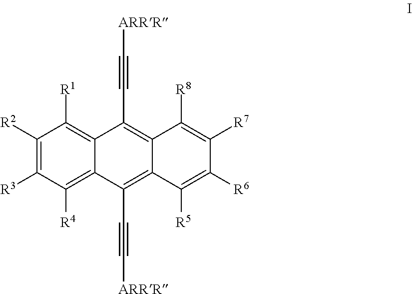
The invention relates to novel non-linear acene derivatives, methods of their preparation, their use as semiconductors in organic electronic (OE) devices, and to OE devices comprising these derivatives.

Description

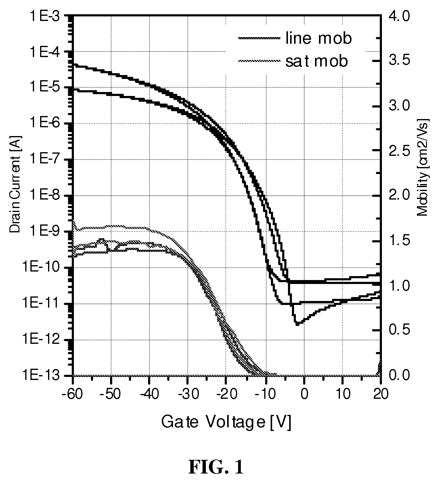
FIELD OF THE INVENTION[0001]The invention relates to novel non-linear acene derivatives, methods of their preparation, their use as semiconductors in organic electronic (OE) devices, and to OE devices comprising these derivatives.BACKGROUND AND PRIOR ART[0002]In recent years, there has been development of organic semiconducting (OSC) materials in order to produce more versatile, lower cost electronic devices. Such materials find application in a wide range of devices or apparatus, including organic field effect transistors (OFETs), organic light emitting diodes (OLEDs), photodetectors, organic photovoltaic (OPV) cells, sensors, memory elements and logic circuits to name just a few. The organic semiconducting materials are typically present in the electronic device in the form of a thin layer, for example less than 1 micron thick.[0003]The performance of OFET devices is principally based upon the charge carrier mobility of the semiconducting material and the current on / off ratio, so ...

Claims


Application Information

Patent Timeline
IPC IPC(8): H01L51/00
CPCC07F7/0809C07F7/0812C07F7/0818Y02E10/549H01L51/0074H01L51/0094H01L51/0558H01L51/0055C07F7/081C07F7/0805H10K85/623H10K85/6576H10K85/40H10K10/484C07F7/08H10K99/00
Inventor MITCHELL, WILLIAMWANG, CHANGSHENGD'LAVARI, MANSOORBLOUIN, NICOLASTIERNEY, STEVEN
Owner MERCK PATENT GMBH
Why Eureka
Try Eureka