

Group iii nitride semiconductor substrate and method for producing the same, and semiconductor light-emitting device and method for producing the same
a technology of nitride semiconductor substrate and semiconductor light-emitting device, which is applied in the direction of polycrystalline material growth, chemically reactive gas growth, crystal growth process, etc., can solve the problems of low light-emitting efficiency, undesirable effects, and inability to obtain crystals with good performance, etc., to achieve high light-emitting intensity, excellent durability, and high light-emitting efficiency
- Summary
- Abstract
- Description
- Claims
- Application Information
AI Technical Summary
Benefits of technology
Problems solved by technology
Method used
Image

Examples
production example 1
[0120](Substrate Production Example 1)
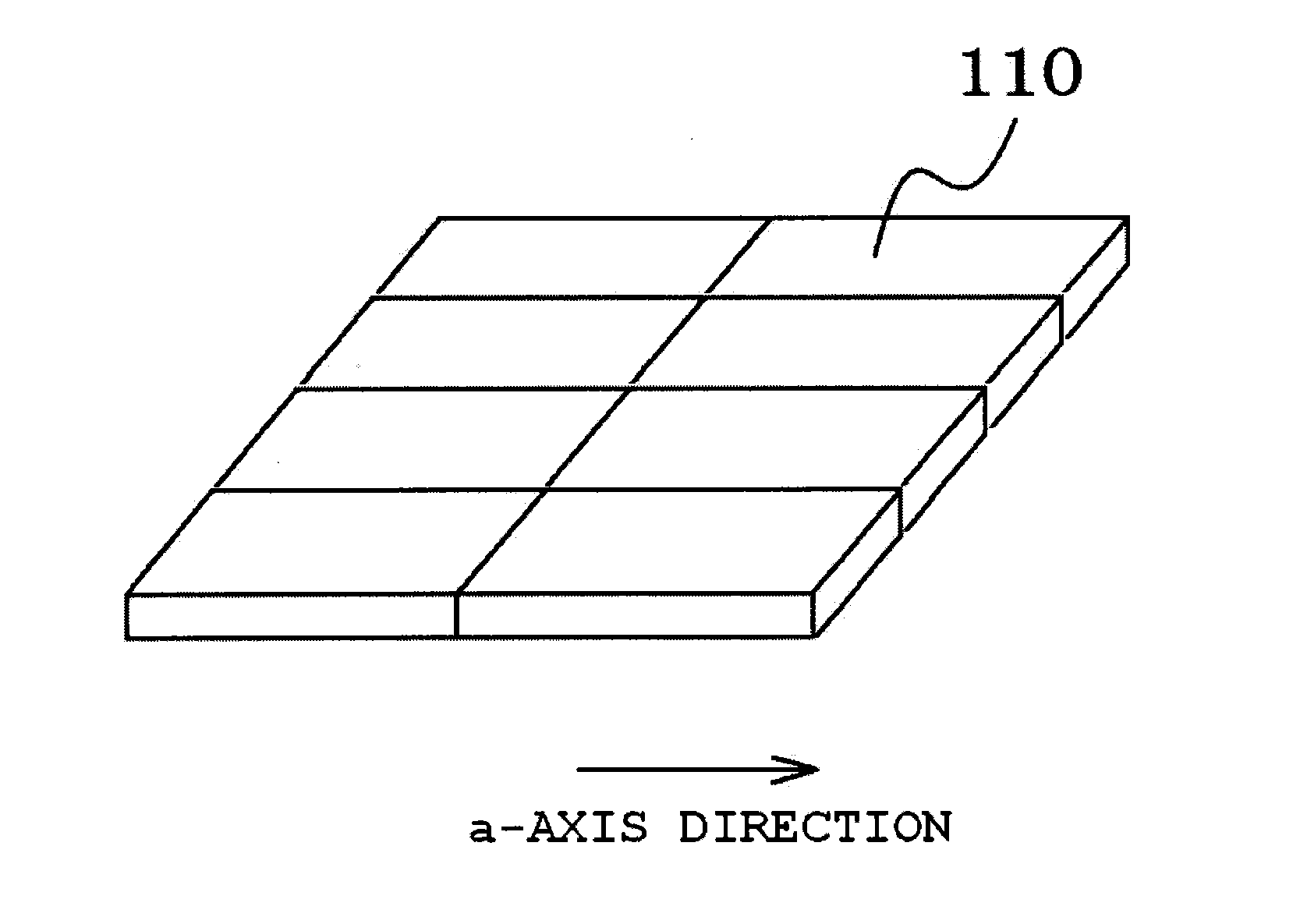
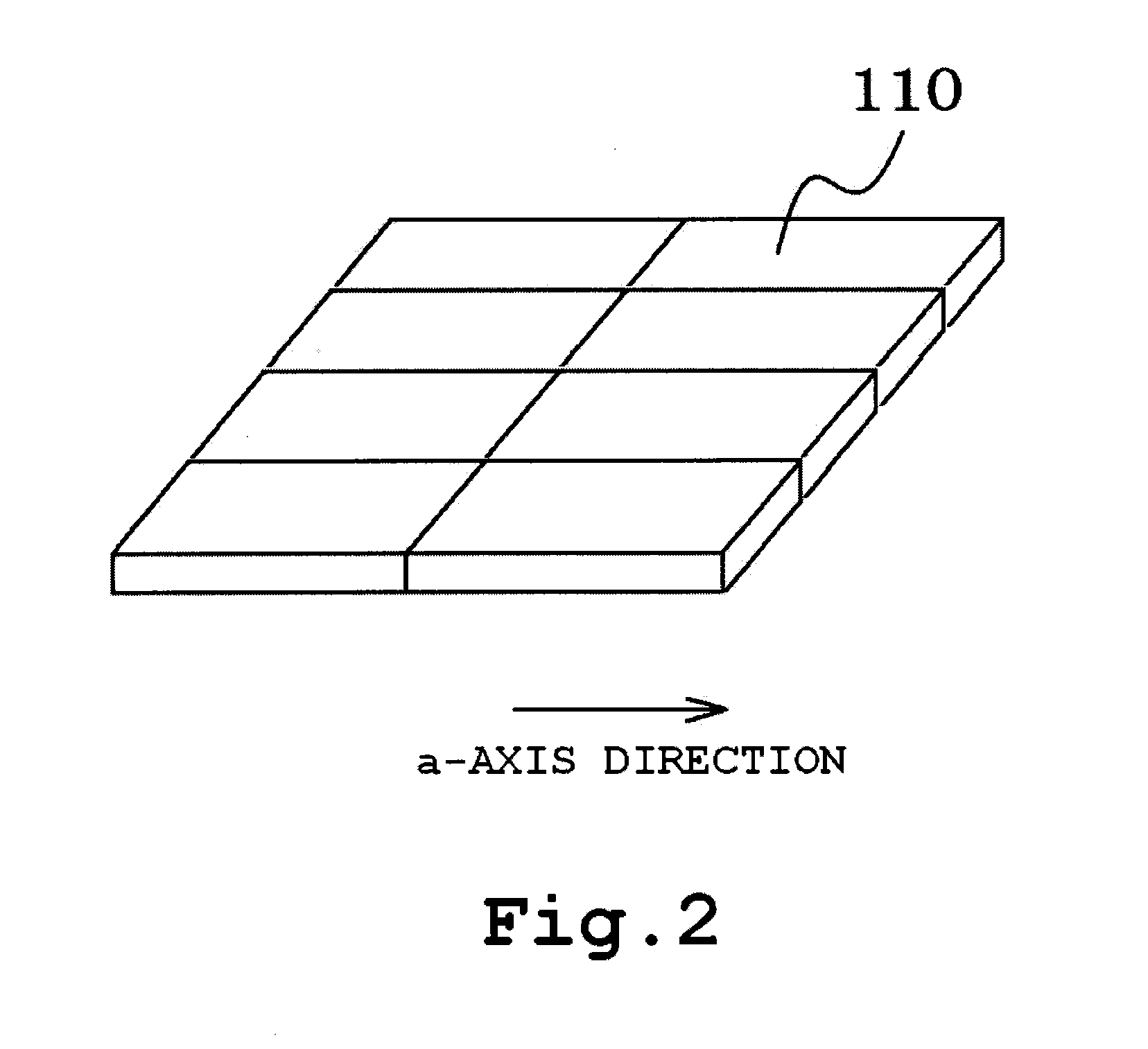
[0121]Eight rectangular free-standing GaN substrates having a principal plane with a 1° off-angle in (c-axis) direction from (20-21) plane were sliced from a GaN crystal ingot fabricated by (0001) plane growth. The free-standing GaN substrates were each cut to dimensions of 30 mm in (a-axis) direction and 17 mm in a direction orthogonal to the a-axis within the principal plane. The distribution of plane directions among the free-standing GaN substrates was within ±0.15°. Using these free-standing GaN substrates as the seeds, the substrates were arranged on a susceptor into two rows in (a-axis) direction and four rows in a direction orthogonal to the a-axis in such a way as to align (c-axis) directions among the free-standing GaN substrates to an accuracy of ±0.25° (see FIG. 2). The sum (Sa) of the contact distances between the edges in the direction of the line of intersection between the principal plane and the C plane was 180 mm, and the s...
production example 2
[0123](Substrate Production Example 2)
[0124]Following the same procedure as in Substrate Production Example 1, a GaN crystal was grown on eight rectangular free-standing GaN substrates having a principal plane with a 1° off-angle in (c-axis) direction from (20-21) plane. The sum (Sa) of the contact distances between the edges in the direction of the line of intersection between the principal plane and the C plane was 180 mm, and the sum (Sc) of the distances between other edges were was 68 mm. The amount of fall in temperature during growth was less than 5° C. The resulting GaN crystal was sliced by cutting with a wire, shaped by dicing, and also polished using diamond abrasive and surface polished by CMP, thereby producing 400 μm thick square-shaped free-standing GaN substrates which measured 55 mm on a side and whose principal plane was (20-21) plane. The tilt angle distributions in (a-axis) direction and in a direction orthogonal to the a-axis within the plane of the substrate ...
production example 7
[0134](Substrate Production Example 7)
[0135]Eight free-standing GaN substrates having principal planes with off-angles of from −1° to 1° in (a-axis) direction from (20-21) plane were prepared. These free-standing GaN substrates were arranged as seeds on a susceptor in two rows in (a-axis) direction and four rows in a direction orthogonal to the a-axis, in such a way as to align (c-axis) directions among the free-standing GaN substrates to an accuracy of ±0.25°. The substrates were arranged on the susceptor with those substrates having a −1° off-angle being placed on side, and those substrates having a 1° off-angle being placed on side. The sum (Sa) of the contact distances between the edges in the direction of the line of intersection between the principal plane and the C plane was 180 mm, and the sum (Sc) of the contact distances between edges other than these was 68 mm. The amount of fall in temperature during growth was less than 5° C. Using the crystal production equipment ...
PUM
 Abstract
Description
Claims
Application Information