Novel liquid crystal display device and useful liquid crystal composition

a liquid crystal display and liquid crystal composition technology, applied in liquid crystal compositions, instruments, chemistry apparatuses and processes, etc., can solve the problems of slow response speed, unsatisfactory response speed and viewing angle characteristics of liquid crystal tvs, and inability to adjust the viewing angle, etc., to improve the response speed, increase the amount of light transmission, and improve the effect of response speed

Active Publication Date: 2013-10-10
DAINIPPON INK & CHEM INC
View PDF2 Cites 19 Cited by
  • Summary
  • Abstract
  • Description
  • Claims
  • Application Information

AI Technical Summary

Benefits of technology

[0015]The present invention is intended to solve the problems described above. That is, it is an object of the invention to provide a liquid crystal display device of the VAIPS mode which uses a liquid crystal material having negative dielectric anisotropy (Δ∈<0), and exhibits a fast response speed, a wide viewing angle, a high transmittance at the time of light transmission, a high black level at the time of light blockage, and an excellent contrast ratio.
[0024]The invention has improved characteristics such as the response speed, amount of light transmission, light leakage caused by an external pressure such as the use of a touch panel, viewing angle and contrast ratio, and has realized a higher response speed, a larger amount of light transmission, a reduction in light leakage caused by an external pressure, a wider viewing angle, and a higher contrast ratio, as compared with liquid crystal display devices produced by the conventional technologies.

Problems solved by technology

However, in order for liquid crystal display television sets to completely replace the conventional television sets utilizing cathode ray tubes (CRT) and to also cope with the demand for 3D imaging or field sequential display, liquid crystal TVs are still not satisfactory in terms of the response speed and viewing angle characteristics.
For example, the IPS mode is excellent in the viewing angle characteristics, but is not satisfactory in terms of the response speed; and the VA mode exhibits a relatively fast response speed, but is not satisfactory in terms of the viewing angle characteristics.
However, there are limitations in overcoming the limit of the response speed that is intrinsic to a liquid crystal material, if amelioration is made only in terms of the electronic circuit of these liquid crystal display devices.
In this mode, it is possible to improve the viewing angle characteristics; however, since it is required to produce liquid crystal cells that have a complicated structure uniformly in order to achieve pixel partitioning, a decrease in production efficiency has been unavoidable.
However, in the VAIPS mode, since the physical behavior of liquid crystal molecules is different from the conventional method for driving a liquid crystal display device, it is required to select a liquid crystal material under a criterion different from the conventional criteria in connection with the liquid crystal material.
However, in the VAIPS mode, since these general calculation formulas do not fit, and no criteria for selecting the liquid crystal material are available, there has been no progress in the improvement of performance, and consequently, application thereof into liquid crystal display devices has been delayed.
However, the liquid crystal composition described in the relevant reference document uses a cyano-based compound, and therefore, the liquid crystal composition is not suitable for active matrix applications.
On the other hand, liquid crystal display devices also have a problem of aiming to achieve mega contrast (CR) by enhancing the black level with a bright luminance.
Furthermore, there is also a demand for a display which is not easily brought into disorder even under a pressing pressure in a touch panel system.

Method used


Image

  • Novel liquid crystal display device and useful liquid crystal composition
  • Novel liquid crystal display device and useful liquid crystal composition
  • Novel liquid crystal display device and useful liquid crystal composition

Examples


example 1

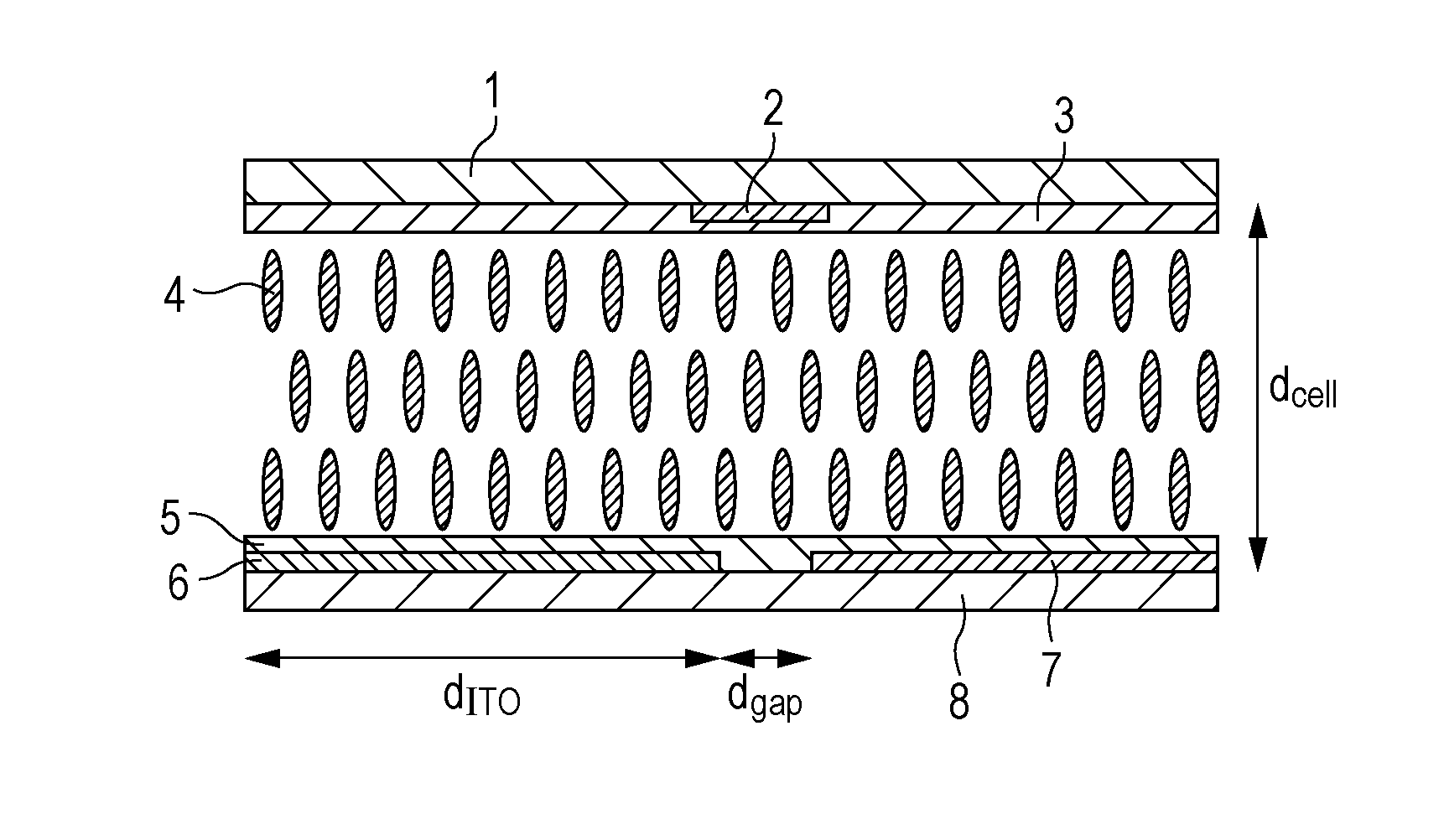
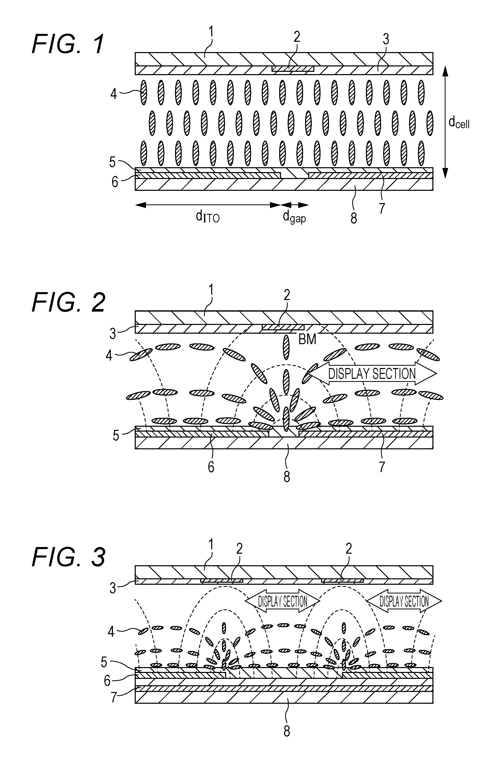
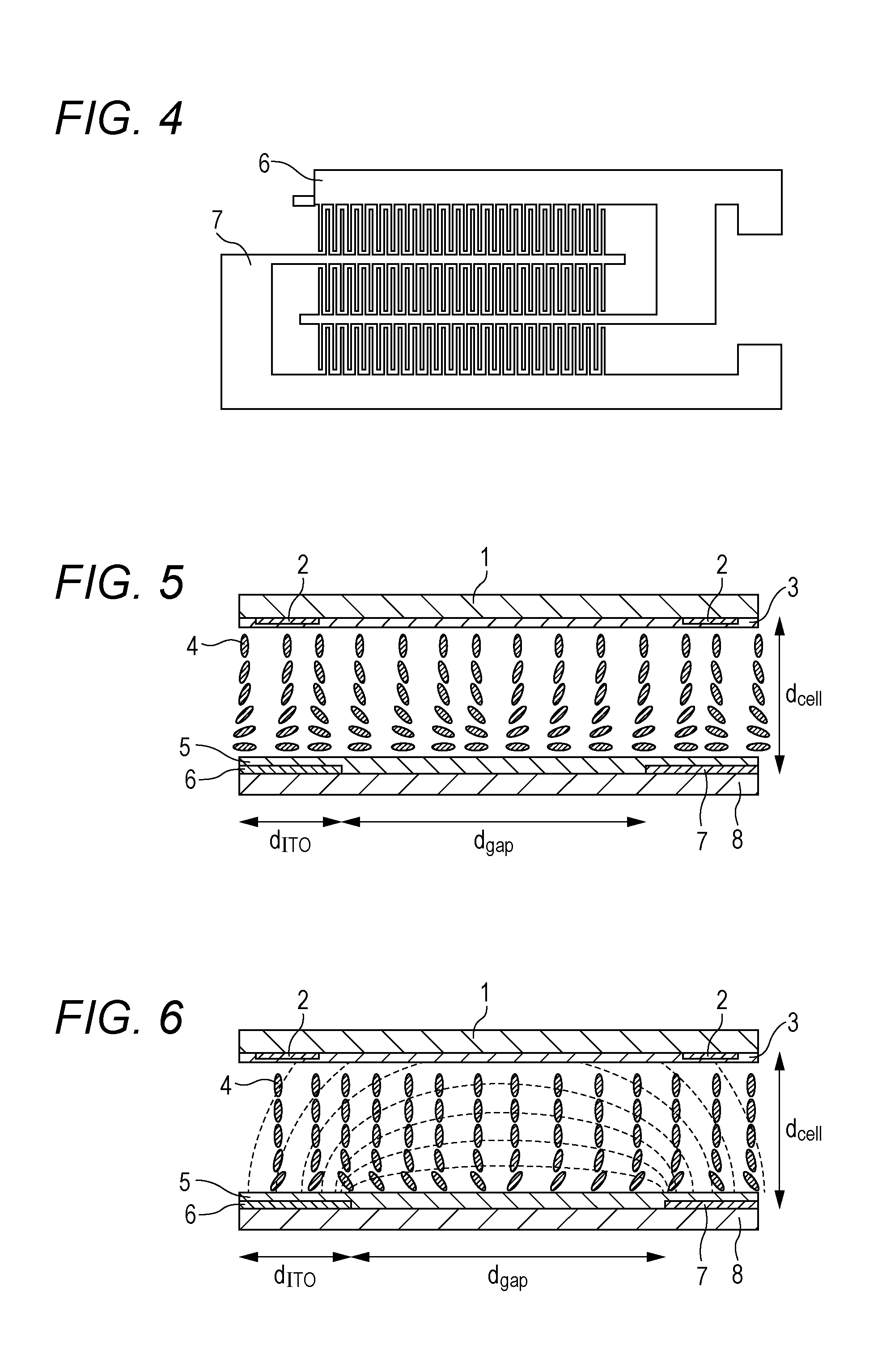
[0075]An electrode structure such as illustrated in FIG. 4 was produced on a second substrate, and a first substrate having no electrode structure provided thereon was used. An alignment film of vertical alignment was formed on each of the respective surfaces that faced each other. The liquid crystals having negative dielectric anisotropy indicated as Example 1 in Table 1 were interposed between the first substrate and the second substrate, and thus a liquid crystal display device was produced (cell thickness: 4.0 μm, alignment film: SE-5300).

example 2

[0078]An electrode structure such as illustrated in FIG. 4 was produced on a second substrate, and a first substrate having no electrode structure provided thereon was used. An alignment film of vertical alignment was formed on each of the other sides of the respective surfaces that faced each other, and an alignment film of horizontal orientation was formed on each of the reverse sides. The liquid crystals having negative dielectric anisotropy indicated as Example 2 in Table 1 were interposed between the first substrate and the second substrate, and thus a liquid crystal display device was produced (cell thickness: 4.0 μm, alignment films: SE-5300, AL-1051). The liquid crystal display device realized a higher response speed, a larger amount of light transmission, a reduction in light leakage caused by external pressure, a wider viewing angle, and a higher contrast ratio, as compared with a conventional VA liquid crystal display device in which the same liquid crystals having negati...

example 3

[0079]An electrode structure such as illustrated in FIG. 4 was produced on a second substrate, and a first substrate having no electrode structure provided thereon was used. An alignment film of vertical alignment was formed on each of the respective surfaces that faced each other. The liquid crystals having negative dielectric anisotropy indicated as Example 3 in Table 1 and 0.3% by mass of 2-methylacrylic acid 4′-{2-[4-(2-acryloyloxyethyl)phenoxycarbonyl]ethyl}biphenyl-4-yl ester were interposed between the first substrate and the second substrate, and thus a liquid crystal display device was produced (cell thickness: 4.0 μm, alignment film: SE-5300). While a driving voltage was applied between the electrodes, ultraviolet radiation was irradiated for 600 seconds (3.0 J / cm2), and thus a polymerization treatment was carried out.

[0080]The liquid crystal display device realized a higher response speed, a larger amount of light transmission, a reduction in light leakage caused by exter...


PUM

PropertyMeasurementUnit
viscosityaaaaaaaaaa
tilt angleaaaaaaaaaa

Abstract

Provided is a liquid crystal display device of VAIPS mode, which uses a liquid crystal material having negative dielectric anisotropy (Δ∈<0), and has a high response speed, a wide viewing angle, a high transmittance at the time of light transmission, a high black level at the time of light blockage, and an excellent contrast ratio. Disclosed is a liquid crystal display device including a first substrate, a second substrate, and a liquid crystal composition layer having negative dielectric constant, which is interposed between the first substrate and the second substrate, the liquid crystal display device being an electro-optical display device which has a plurality of pixels, and in which each of the pixels is independently controllable and has a pair of a pixel electrode and a common electrode, the two electrodes are provided on at least one substrate of the first substrate and the second substrate, and the long axis of the liquid crystal molecules of the liquid crystal composition layer is in a substantial vertical alignment or a hybrid alignment with respect to the substrate surface.

Description

BACKGROUND OF THE INVENTION[0001]1. Field of the Invention[0002]The present invention relates to a liquid crystal display device which uses a nematic crystal composition having negative dielectric anisotropy.[0003]2. Description of the Related Art[0004]Currently, regarding the devices of the active matrix drive system, display modes such as an optically compensated bend (OCB) mode, a vertical alignment (VA) mode and an in-plane switching (IPS) mode have been applied, due to their display quality, to portable terminals, liquid crystal TV sets, projectors, computers, and the like. Since an active matrix display system has a non-linear circuit provided for each pixel, and it has been suggested to use a thin film transistor (TFT) using amorphous silicon or polysilicon, or an organic semiconductor material. Furthermore, as a method for the alignment of liquid crystal molecules to cope with an increase in display size or high definition display, it has been suggested to use a photo-alignm...

Claims


Application Information

Patent Timeline
Patent Type & Authority Applications(United States)
IPC IPC(8): G02F1/1337
CPCC09K19/3066C09K2019/301C09K19/3402C09K19/42C09K2019/0466C09K2019/3037C09K2019/304C09K2019/3425G02F1/134363G02F2001/13712G02F1/133711G02F1/133723C09K2019/3004C09K2019/3009C09K19/322G02F1/13712C09K19/12C09K19/30G02F1/1337G02F1/1343C09K2019/0448
Inventor TAKEUCHI, KIYOFUMIKANEOYA, MASAKAZU
Owner DAINIPPON INK & CHEM INC
Why Eureka
Try Eureka