Semiconductor device and method for manufacturing semiconductor device

a semiconductor and semiconductor film technology, applied in the direction of semiconductor devices, electrical devices, transistors, etc., can solve the problems of increased power consumption, reduced resistance of oxide semiconductor films, poor electrical characteristics of transistors, etc., and achieve excellent electrical characteristics, reduce the amount of oxygen vacancies in oxide semiconductor films, and reduce the effect of plasma damage to oxide semiconductor films

Active Publication Date: 2013-10-17
SEMICON ENERGY LAB CO LTD
View PDF21 Cites 85 Cited by
  • Summary
  • Abstract
  • Description
  • Claims
  • Application Information

AI Technical Summary

Benefits of technology

[0025]An oxide semiconductor film is exposed to plasma generated in an oxidizing atmosphere to supply oxygen to the oxide semiconductor film, whereby the amount of oxygen vacancies in the oxide semiconductor film can be reduced. Further, when a first insulating film which is dense and hard is formed immediately after the plasma treatment is performed, the concentration of impurities at the interface between the oxide semiconductor film and the first insulating film can be reduced. Furthermore, with the formation of the first insulating film which is dense and hard, the oxide semiconductor film can be prevented from being exposed to plasma and plasma damage to the oxide semiconductor film can be reduced during later film formation of a second insulating film. Accordingly, ac

Problems solved by technology

In a transistor including an oxide semiconductor, oxygen vacancies in an oxide semiconductor film cause the transistor to have poor electrical characteristics.
This is because charge is generated owing to the oxygen vacancies in the oxide semiconductor film, result

Method used


Image

  • Semiconductor device and method for manufacturing semiconductor device
  • Semiconductor device and method for manufacturing semiconductor device
  • Semiconductor device and method for manufacturing semiconductor device

Examples


embodiment 1

[0059]In this embodiment, a semiconductor device of one embodiment of the present invention and a method for manufacturing the semiconductor device will be described with reference to drawings.

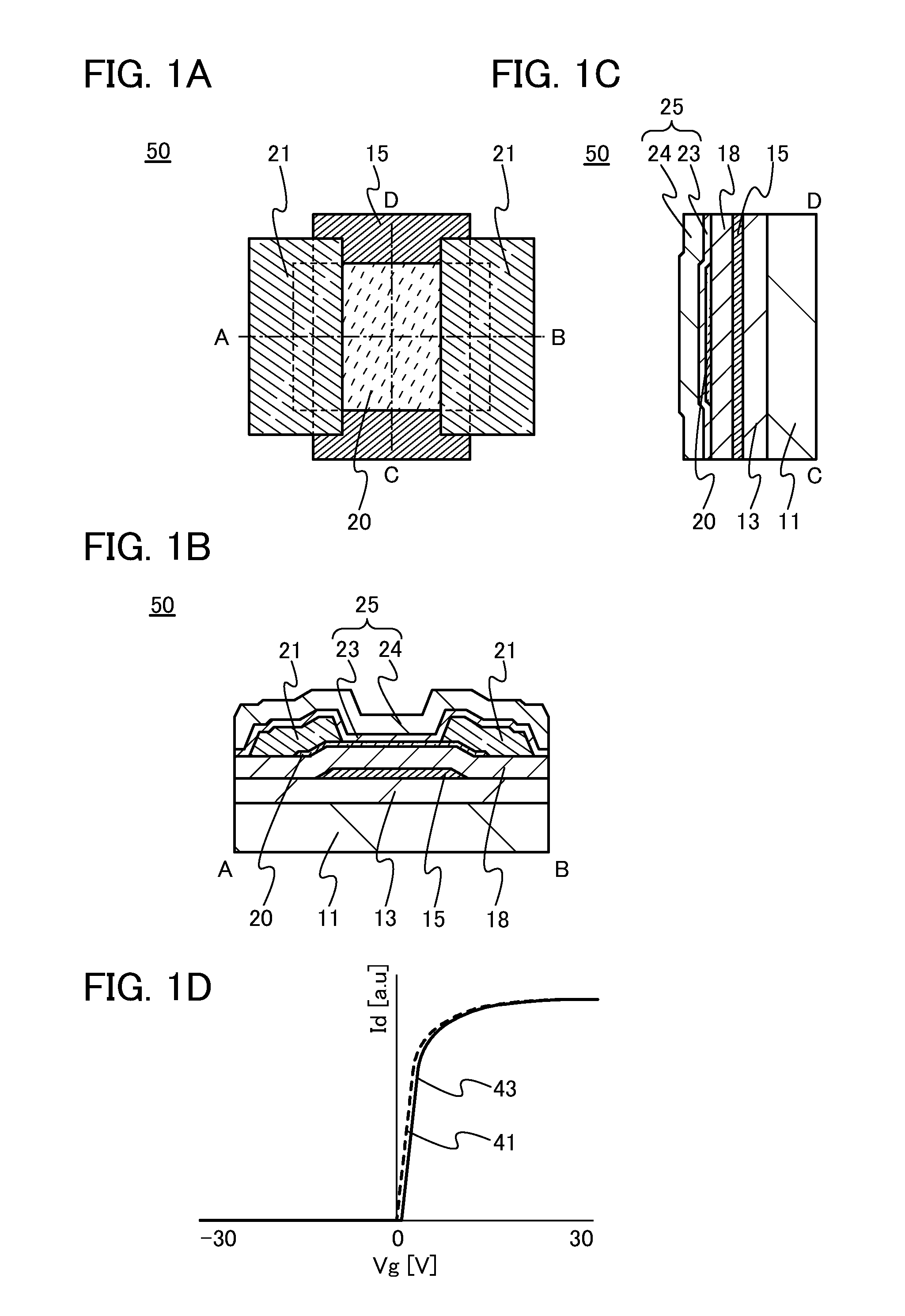
[0060]FIGS. 1A to 1C are a top view and cross-sectional views of a transistor 50 of a semiconductor device. FIG. 1A is a top view of the transistor 50, FIG. 1B is a cross-sectional view taken along dashed-dotted line A-B in FIG. 1A, and FIG. 1C is a cross-sectional view taken along dashed-dotted line C-D in FIG. 1A. Note that in FIG. 1A, some components of the transistor 50 (e.g., a gate insulating film 18), a substrate 11, a base insulating film 13, an insulating film 23, an insulating film 24, and the like are omitted for simplicity.

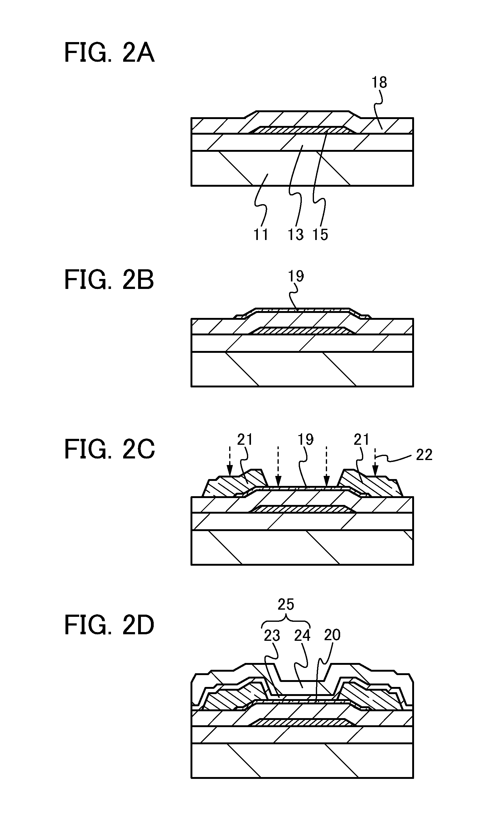
[0061]The transistor 50 illustrated in FIGS. 1B and 1C includes a gate electrode 15 over the base insulating film 13. Moreover, the gate insulating film 18 over the base insulating film 13 and the gate electrode 15, an oxide semiconductor film 20 overlapping with...

embodiment 2

[0179]In this embodiment, a structure and a method for manufacturing a transistor whose gate insulating film is different from that of the transistor shown in Embodiment 1 will be described with reference to FIGS. 1A to 1C and FIG. 3.

[0180]As the gate insulating film 18 illustrated in FIGS. 1A to 1C, in a transistor of this embodiment, a dense and hard oxide insulating film into which and from which oxygen is diffused, typically, a silicon oxide film or a silicon oxynitride film having an etching rate lower than or equal to 10 nm / min, preferably lower than or equal to 8 nm / min when etching is performed at 25° C. with 0.5 weight % of hydrofluoric acid is formed.

[0181]Note that in the case where the dense and hard oxide insulating film into which and from which oxygen is diffused is formed as the gate insulating film 18, a silicon oxide film or a silicon oxynitride film is formed under the following conditions in a manner similar to that of the insulating film 23 of Embodiment 1: the ...

embodiment 3

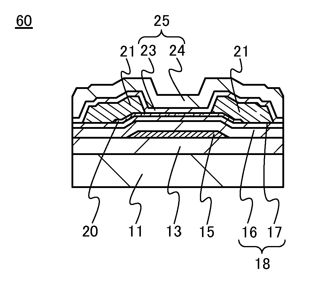
[0195]In this embodiment, a transistor having a structure different from that of Embodiment 1 and Embodiment 2 will be described with reference to FIG. 4. A transistor 70 of this embodiment includes a plurality of gate electrodes facing each other with an oxide semiconductor film provided therebetween.

[0196]A transistor 70 illustrated in FIG. 4 includes the base insulating film 13 over the substrate 11 and the gate electrode 15 over the base insulating film 13. Moreover, the gate insulating film 18 over the base insulating film 13 and the gate electrode 15, the oxide semiconductor film 20 overlapping with the gate electrode 15 with the gate insulating film 18 provided therebetween, and the pair of electrodes 21 in contact with the oxide semiconductor film 20 are included. The protective film 25 including the insulating film 23 and the insulating film 24 is over the gate insulating film 18, the oxide semiconductor film 20, and the pair of electrodes 21. Further, a gate electrode 61 o...


PUM


Abstract

In a semiconductor device including an oxide semiconductor, the amount of oxygen vacancies is reduced. Moreover, electrical characteristics of a semiconductor device including an oxide semiconductor are improved. The semiconductor device includes a transistor including a gate electrode over a substrate, a gate insulating film covering the gate electrode, an oxide semiconductor film overlapping with the gate electrode with the gate insulating film provided therebetween, and a pair of electrodes in contact with the oxide semiconductor film; and over the transistor, a first insulating film covering the gate insulating film, the oxide semiconductor film, and the pair of electrodes; and a second insulating film covering the first insulating film. An etching rate of the first insulating film is lower than or equal to 10 nm/min and lower than an etching rate of the second insulating film when etching is performed at 25° C. with 0.5 weight % of hydrofluoric acid.

Description

BACKGROUND OF THE INVENTION[0001]1. Field of the Invention[0002]The present invention relates to a semiconductor device including a transistor.[0003]2. Description of the Related Art[0004]Transistors used for most flat panel displays typified by a liquid crystal display device or a light-emitting display device are formed using a silicon semiconductor such as amorphous silicon, single crystal silicon, or polycrystalline silicon provided over a glass substrate. Further, transistors formed using such silicon semiconductors are used in integrated circuits (ICs) and the like.[0005]In recent years, attention has been drawn to a technique in which, instead of a silicon semiconductor, a metal oxide exhibiting semiconductor characteristics is used for transistors. Note that in this specification, a metal oxide exhibiting semiconductor characteristics is referred to as an oxide semiconductor.[0006]For example, a technique is disclosed in which a transistor is manufactured using zinc oxide or...

Claims


Application Information

Patent Timeline
IPC IPC(8): H01L29/786H01L29/66
CPCH01L29/7869H01L29/66969H01L29/66742H01L29/78606H01L21/0217H01L21/02271H01L21/02565H01L21/47573H01L27/1225H01L27/1259H01L29/78696
Inventor OKAZAKI, KENICHIMIYAMOTO, TOSHIYUKINOMURA, MASAFUMIHAMOCHI, TAKASHIYAMAZAKI, SHUNPEISASAKI, TOSHINARI
Owner SEMICON ENERGY LAB CO LTD
Why Eureka
Try Eureka