

Functionalized Semiconducting Polymers For Use In Organic Photovoltaic Devices
a semiconducting polymer and photovoltaic device technology, applied in semiconductor devices, solid-state devices, nano-informatics, etc., can solve the problems of insufficient cost-effective widespread deployment, insufficient cost-effectiveness of organic photovoltaic devices, and heavy and brittle photovoltaic devices
- Summary
- Abstract
- Description
- Claims
- Application Information
AI Technical Summary
Benefits of technology
Problems solved by technology
Method used
Image

Examples
example 1
Reagents and Physical Measurements
[0084]Triethoxy-2-thienylsilane, EDOT, PSSNa (MW=70 000 Da), dimethyformamide (DMF), tetrahydrofuran (THF), dichloromethane, isopropyl alcohol, and o-dichlorobenzene may be used as commercially available products. P3BHT (Mn=13 300 Da, PDI=1.86) is also commercially available from Polymer Source and may be used without further purification. Regioregular P3HT and PCBM is also commercially available from Rieke Metals and American Dye Source Inc, respectively. A commercially available colloidal suspension of (cPEDOT:PSS)−Na+ is available from H.C. Stark (Heraeus Clevios P VP Al4083). ITO coated glass substrates (8-12 ohms / square are available from Delta Technologies, Ltd. The ITO coated glass substrates were cleaned by sequential 10 min ultrasonication in dichloromethane, water, and isopropyl alcohol, and were further cleaned by exposure to a 10 min air plasma at 0.1 mTorr (Harrick Plasma, PDC 32 G, 18 W) immediately prior to use.
example 2
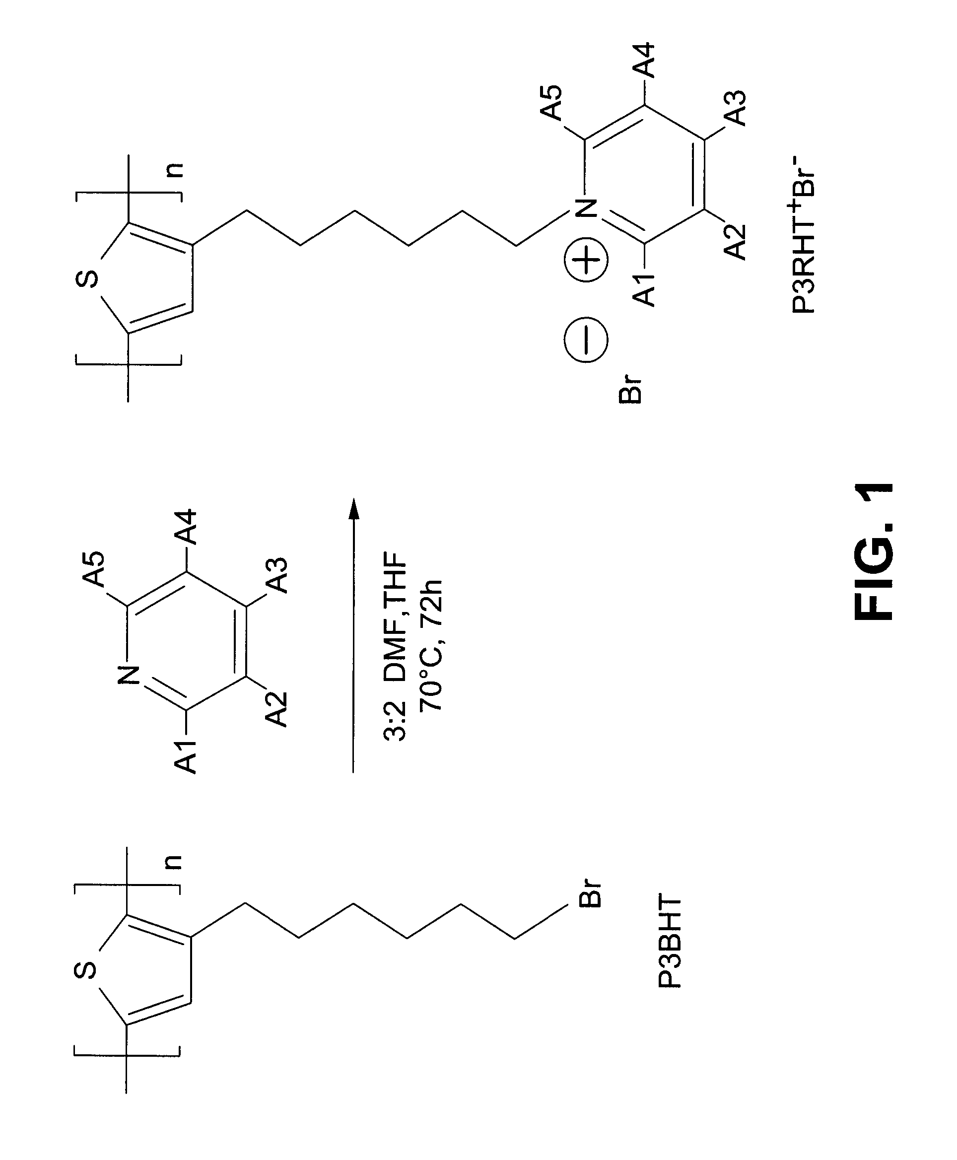
Synthesis of FSPs
[0085]The synthesis is conducted according to a modified protocol of the procedures outlined by Xue et al. and Gutakeret et al. Briefly, and as an example, a functionalized pyridine may be added to a stirred 3:2 (v / v) DMF:THF solution of P3BHT. The mixture is stirred at 70° C. under an Ar atmosphere for 72 h. After removal of most of the solvent, the residue is precipitated in THF (50 mL). The precipitate is collected by centrifuging at 10 000 rpm for 30 min, and the extract dried under vacuum at 50° C. to obtain FSP as a solid.
example 3
Preparation of (FSP / cPEDOT:PSS)n Coated ITO Substrates
[0086]For the deposition of FSP / cPEDOT:PSS bilayers on ITO, a LbL method in air may be used. Freshly cleaned ITO substrates are first immersed in a 95:5 (v / v) H2O:DMF solution of FSP−Br+ for 5 min, rinsed with deionized water, then transferred to a 0.8 wt % aqueous solution of (cPEDOT:PSS)−Na+ for 5 min. Rinsing with deionized water completes one bilayer formation cycle. After performing a chosen number of cycles, completed films are spin dried at 3000 rpm for 60 s.
PUM
| Property | Measurement | Unit |
|---|---|---|
| semiconducting | aaaaa | aaaaa |
| conductive | aaaaa | aaaaa |
| brittle | aaaaa | aaaaa |
Abstract
Description
Claims
Application Information