Heavily doped semiconductor nanoparticles

a technology of semiconductor nanoparticles and doped materials, which is applied in the direction of semiconductor devices, luminescent compositions, chemistry apparatus and processes, etc., can solve the problems of fundamental understanding and elusive doping, and achieve the effect of wide application and enhanced potential application of such materials

Active Publication Date: 2013-11-14
YISSUM RES DEV CO OF THE HEBREWUNIVERSITY OF JERUSALEM LTD +1
View PDF6 Cites 15 Cited by
  • Summary
  • Abstract
  • Description
  • Claims
  • Application Information

AI Technical Summary

Benefits of technology

[0022]Doping of semiconductor materials by impurity atoms enables their widespread application in micro- and optoelectronics. However, for strongly confined colloidal semiconductor nanocrystals, doping has proven elusive. This arises both from the synthetic challenge of how to introduce single impurities and from a lack of fundamental understanding of this heavily doped limit under strong quantum confinement. Herein, provided are heavily doped colloidal semiconductor nanocrystals and a process for their preparation, namely for intentionally introducing (doping) an impurity su

Problems solved by technology

However, for strongly confined colloidal semiconductor nanocrystals, doping has proven elusive.
This arises both from the synthetic challenge o

Method used


Image

  • Heavily doped semiconductor nanoparticles
  • Heavily doped semiconductor nanoparticles
  • Heavily doped semiconductor nanoparticles

Examples


Embodiment Construction

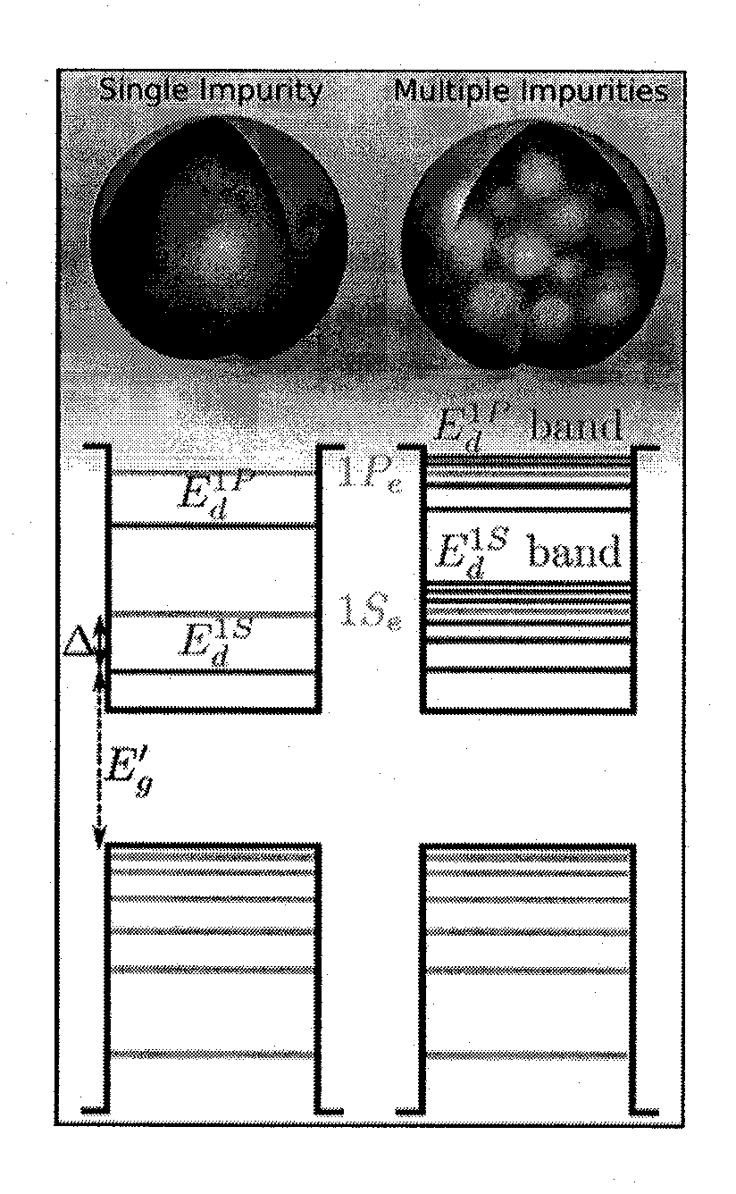
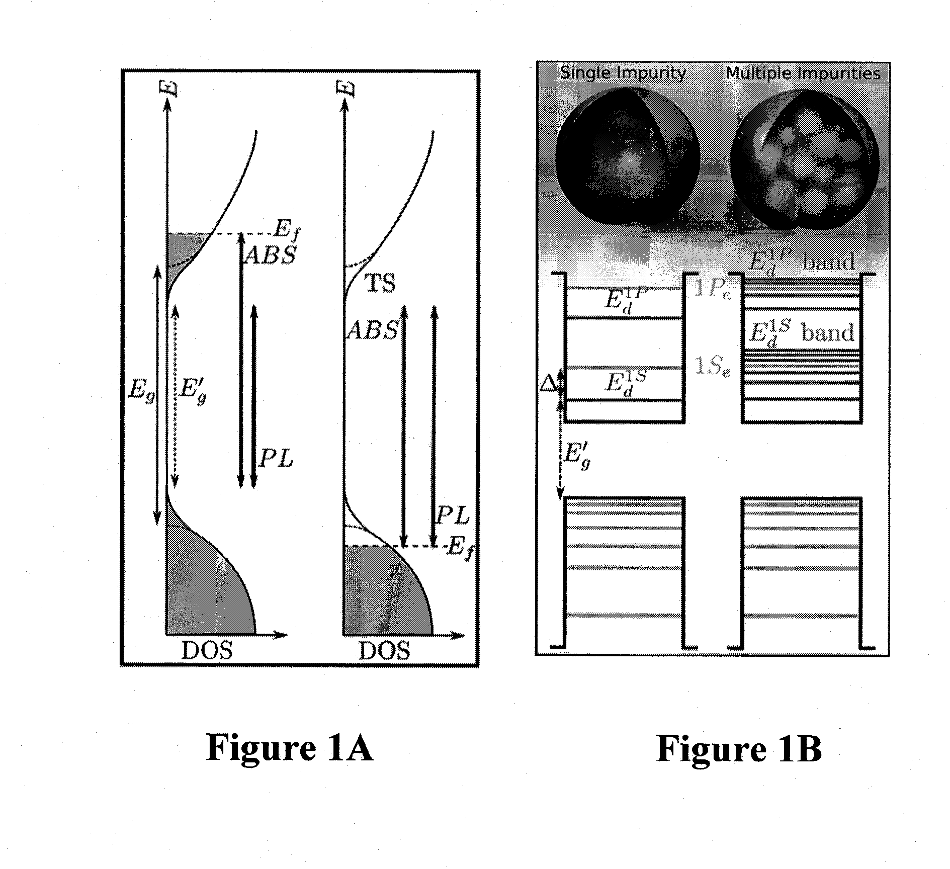
[0135]The invention provides a family of novel doped nanoparticles and a process for their preparation, which permits doping semiconductor nanocrystals with doping atoms, and a specific embodiment relates to metal dopants. By changing the dopant type and concentration, exquisite control of the electronic properties, including the band gap and Fermi energy is achieved. The role of strong quantum confinement leading to localization of impurity levels, as well as disorder effects leading to band-tailing in small nanocrystals, have been studied experimentally and theoretically. The successful controlled doping provides n- and p-doped semiconductor nanocrystals which greatly enhance the potential application of such materials in solar cells, thin-film transistors, and optoelectronic devices.

[0136]The addition of even a single impurity atom to a semiconductor nanocrystal with a diameter of 4 nm, and which contains about 1,000 atoms, leads to a nominal doping level of 7×10¹⁹ atoms per cm3....


PUM


Abstract

Herein, provided are heavily doped colloidal semiconductor nanocrystals and a process for introducing an impurity to semiconductor nanoparticles, providing control of band gap, Fermi energy and presence of charge carriers. The method is demonstrated using InAs colloidal nanocrystals, which are initially undoped, and are metal-doped (Cu, Ag, Au) by adding a metal salt solution.

Description

FIELD OF THE INVENTION[0001]This invention relates to doped semiconductor nanoparticles.BACKGROUND OF THE INVENTION[0002]Doping of bulk semiconductors, the process of intentional introduction of impurity atoms into a crystal discovered back in the 1940s, is a key route for tuning their properties. Its introduction allowed the wide-spread application of semiconductors in electronic and electro-optic components [1]. Controlling the size and dimensionality of semiconductor structures is an additional powerful way to tune their properties via quantum confinement effects. In this respect, colloidal semiconductor nanocrystals have emerged as a family of materials with size dependent optical and electronic properties. Combined with their capability for wet-chemical processing, this has led to nanocrystal-based light emitting diodes, solar cells and transistor devices prepared via facile and scalable bottom-up approaches. Impurity doping in such colloidal nanocrystals still remains an open ...

Claims


Application Information

Patent Timeline
IPC IPC(8): H01L29/06H01L21/22
CPCH01L29/0665H01L21/22B01J13/0039B82Y10/00C09K11/54C09K11/61C09K11/62C09K11/64C09K11/88C09K11/881C09K11/883H01L21/02601H01L29/167H01L29/207H01L29/227H01L29/365H01L33/18
Inventor COHEN, GUYMILLO, ODEDMOCATTA, DAVIDRABANI, ERANBANIN, URI
Owner YISSUM RES DEV CO OF THE HEBREWUNIVERSITY OF JERUSALEM LTD
Why Eureka
Try Eureka