Write control device

a control device and write control technology, applied in static storage, digital storage, instruments, etc., can solve the problems of inability to preserve data in nonvolatile memory devices, and inability to precisely control the phase change resistance cell in program and verify (pnv) operations. , to achieve the effect of reducing the transmission delay of memory cells, improving the phenomenon of write time delay, and stable in a shor

Active Publication Date: 2013-11-21
SK HYNIX INC
View PDF9 Cites 1 Cited by
  • Summary
  • Abstract
  • Description
  • Claims
  • Application Information

AI Technical Summary

Benefits of technology

[0029]Embodiments of the present invention are directed to improving a write time delay phenomenon due to a small write current and large parasitic components on a write path of a cell array having a large size. The present invention provides a write driving unit with an adjusted size ratio of driving transistors, so that the write driving unit may provide a write current that is stabilized in a short time. Also, the driving transistors are over-driven using a voltage drop generated at an output node of the write driving unit for a given time in an initial period of a write operation so as to reduce transmission delay to memory cells. Moreover, diode-coupled transistors, coupled to the driving transistors, are turned on due to the voltage drop so as to reduce the transmission delay.

Problems solved by technology

However, unlike a volatile RAM device, a nonvolatile memory device preserves data even when a power source is off.
However, for example, if a reference current, which is used to generate the set write current and is received from the outside or generated inside the chip, changes by some factors or if a clock having a wrong value is generated by mismatched circuits, the set write current may be generated with an undesired quenching slope.
Moreover, without accurately checking the quenching slope, it is impossible to precisely control the phase change resistance cell in program and verify (PNV) operations and a multi-level cell MLC where multi-leveled resistance distribution of a phase change material, e.g., germanium antimony tellurium (GST), is formed.
However, it takes a much longer time to supply cells with the write current when using a small current value than when using a large current value.
That is, when the write driving unit supplies a small write current to the cells, it takes much longer to supply the current because of parasitic components on a write path.
In addition, there is a time delay due to parasitic components on a write path.
As the size of the cell array becomes larger, the delay time occurring due to the parasitic components on the write path also become greater.
A conventional write driving unit has not introduced improvements to such a write time delay phenomenon.

Method used


Image

  • Write control device
  • Write control device
  • Write control device

Examples


Embodiment Construction

[0053]Exemplary embodiments of the present invention will be described in detail with reference to the attached drawings.

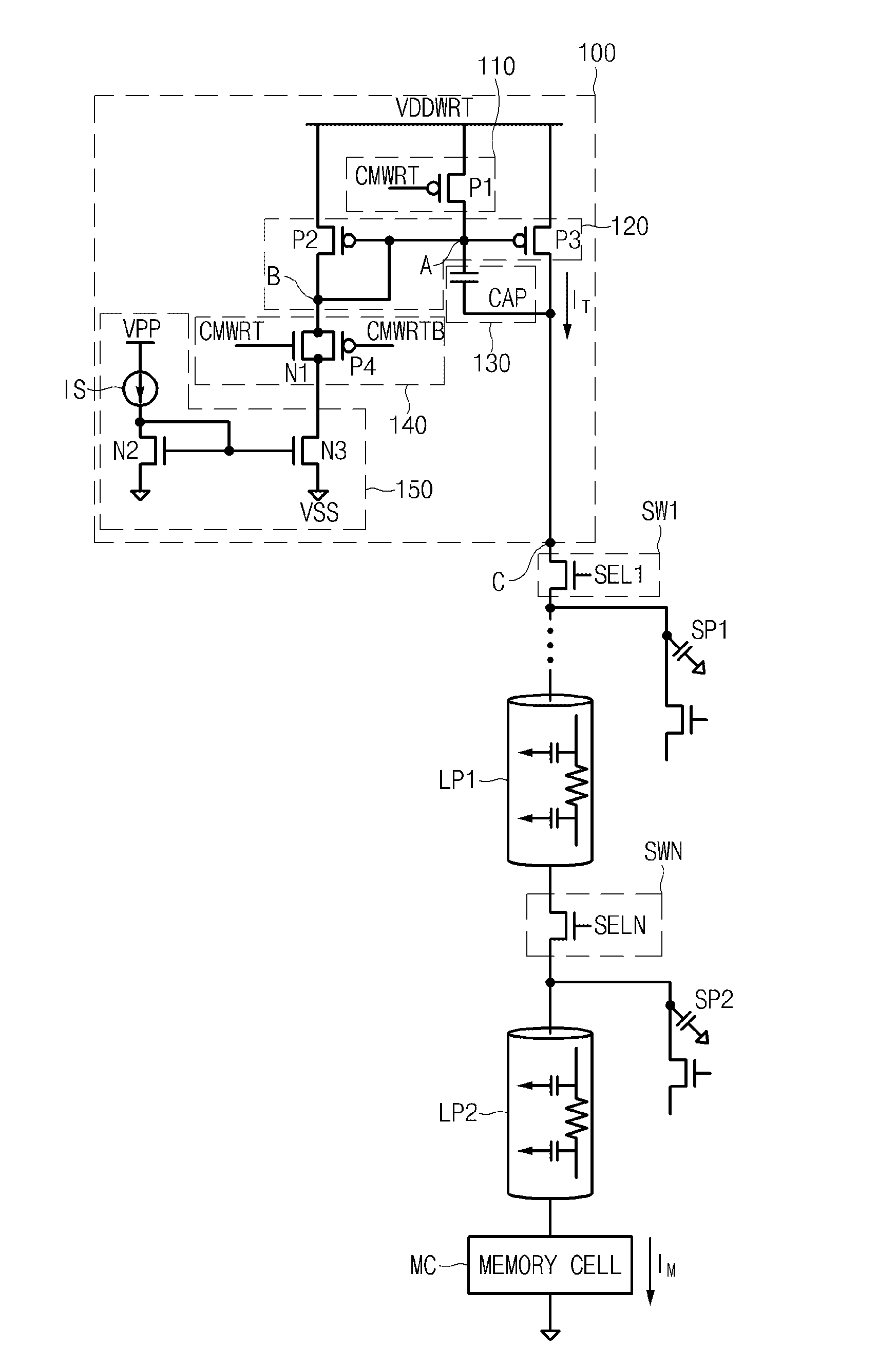
[0054]FIG. 5 illustrates a write control device according to an embodiment of the present invention.

[0055]Referring to FIG. 5, the write control device includes a write driving unit 100. The write driving unit 100 is coupled to a memory cell MC through a plurality of selection switches SW1˜SWN and supplies a driving current to the memory cell MC.

[0056]The write driving unit 100 includes a voltage supply unit 110, a driving unit 120, an over-driving control unit 130, a switching unit 140, and a current supply unit 150.

[0057]The voltage supply unit 110 includes a PMOS transistor P1 coupled to and disposed between a power voltage (VDDWRT) terminal and a node A. The PMOS transistor P1 has a gate to receive a driving control signal CMWRT.

[0058]The driving unit 120 includes PMOS transistors P2 and P3. The PMOS transistor P2 is coupled to and disposed between the power v...


PUM


Abstract

A write control device includes a switching unit configured to selectively supply a write current in response to a driving control signal, a driving unit configured to supply a driving current to a memory cell corresponding to the write current applied through the switching unit, and an over-driving control unit coupled to an output node of the driving unit and configured to over-drive the output node in response to the driving control signal.

Description

CROSS-REFERENCE TO RELATED APPLICATION[0001]The priority of Korean patent application No. 10-2012-0053895 filed on May 21, 2012, the disclosure of which is hereby incorporated in its entirety by reference, is claimed.BACKGROUND OF THE INVENTION[0002]The present invention relates to a write control device, and more specifically, to a technology for rapidly performing a write operation of a nonvolatile memory device configured to sense data based on resistance change.[0003]Generally, memory devices may be classified as volatile memory devices or nonvolatile memory devices. A nonvolatile memory device includes a nonvolatile memory cell capable of preserving stored data even when a power source is off. A nonvolatile memory device may be implemented, for example, as a flash random access memory (RAM) device, a phase change RAM (PCRAM) device, or the like.[0004]PCRAM devices include memory cells that are implemented using a phase change material, for example, germanium antimony tellurium ...

Claims


Application Information

Patent Timeline
Patent Type & Authority Applications(United States)
IPC IPC(8): G11C7/00
CPCG11C13/0004G11C13/0038G11C13/0061G11C13/0069G11C2013/0092G11C13/00G11C16/10G11C16/30
Inventor OH, BYOUNG CHANSHIN, YOON JAE
Owner SK HYNIX INC
Why Eureka
Try Eureka