Nitride semiconductor device and manufacturing method thereof

Active Publication Date: 2013-11-28
ROHM CO LTD
View PDF9 Cites 30 Cited by
  • Summary
  • Abstract
  • Description
  • Claims
  • Application Information

AI Technical Summary

Benefits of technology

The present invention provides a nitride semiconductor device with a good boundary between the nitride semiconductor and the gate insulating film, which improves device performance. The method uses a passivation film with an opening formed through etching that prevents damage to the surface of the electron supply layer and avoids exposure to air. This results in a nitride semiconductor device with excellent characteristics.

Problems solved by technology

As a result, damage to the surface of the AlGaN layer due to etching is unavoidable.
Thus, the boundary between the AlGaN layer and the gate insulating layer is not necessarily in a good state, which presents a problem in that it is difficult to attain excellent device characteristics.

Method used


Image

  • Nitride semiconductor device and manufacturing method thereof
  • Nitride semiconductor device and manufacturing method thereof
  • Nitride semiconductor device and manufacturing method thereof

Examples


embodiment 1

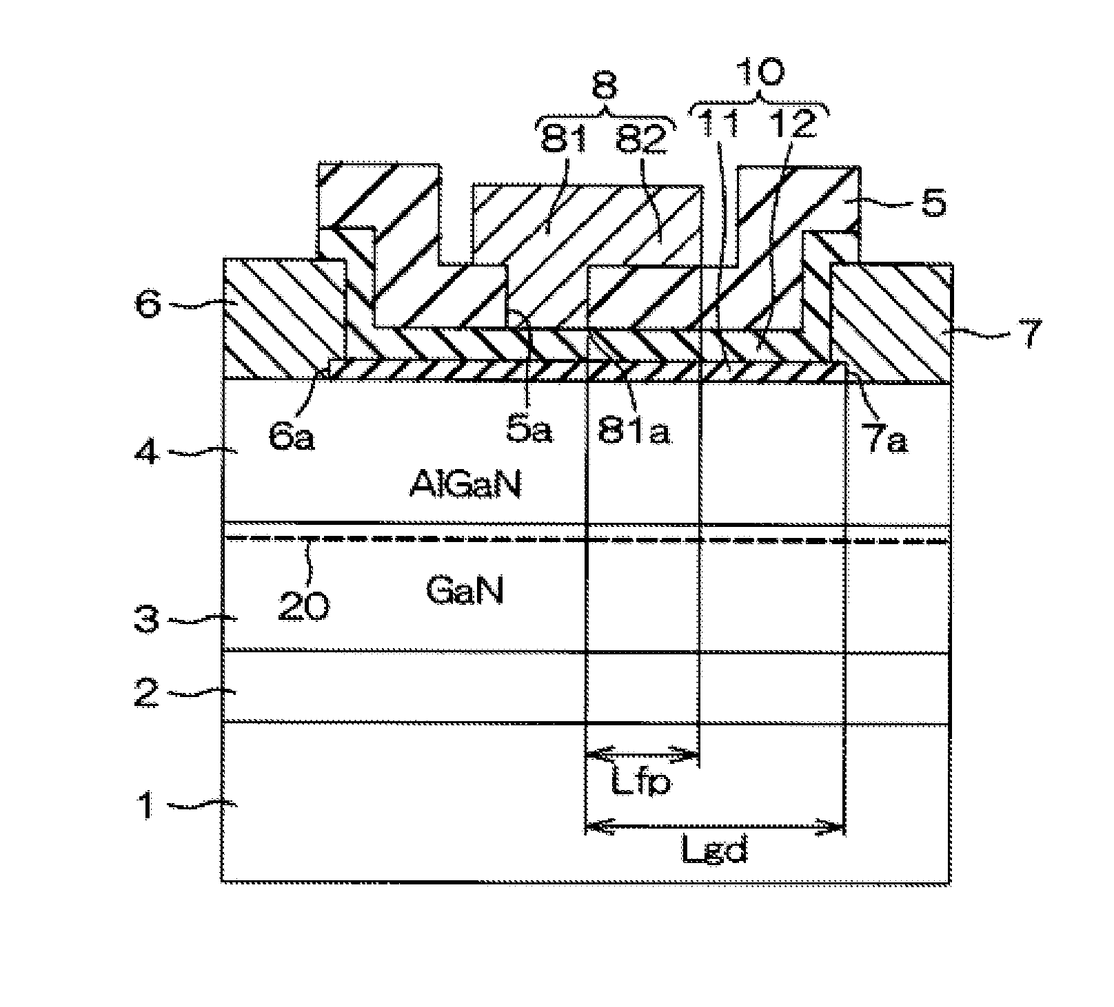
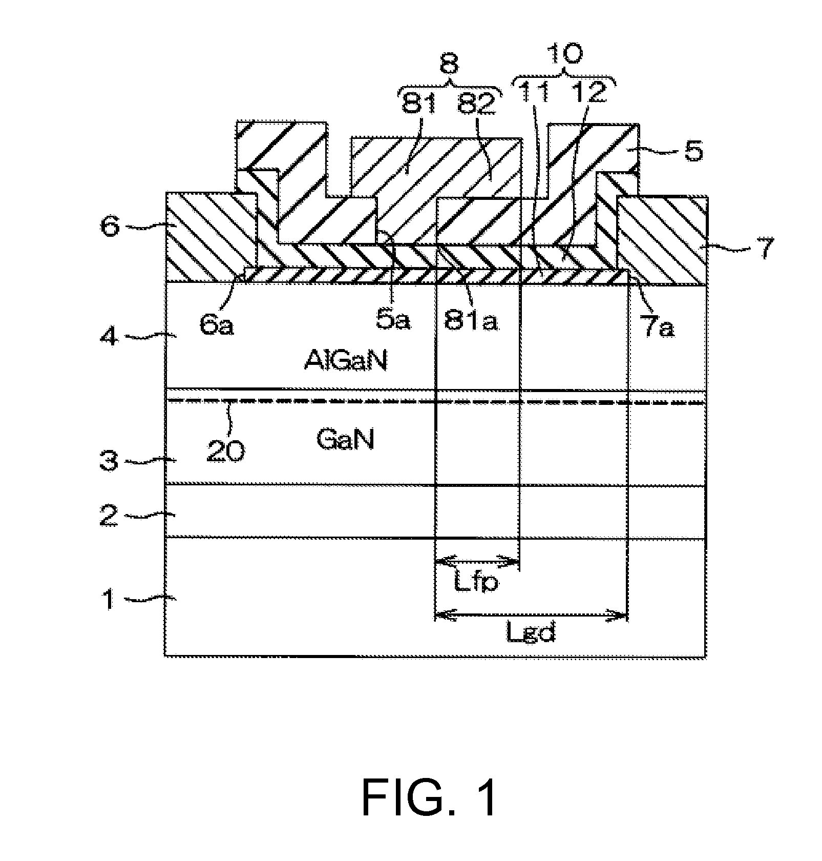
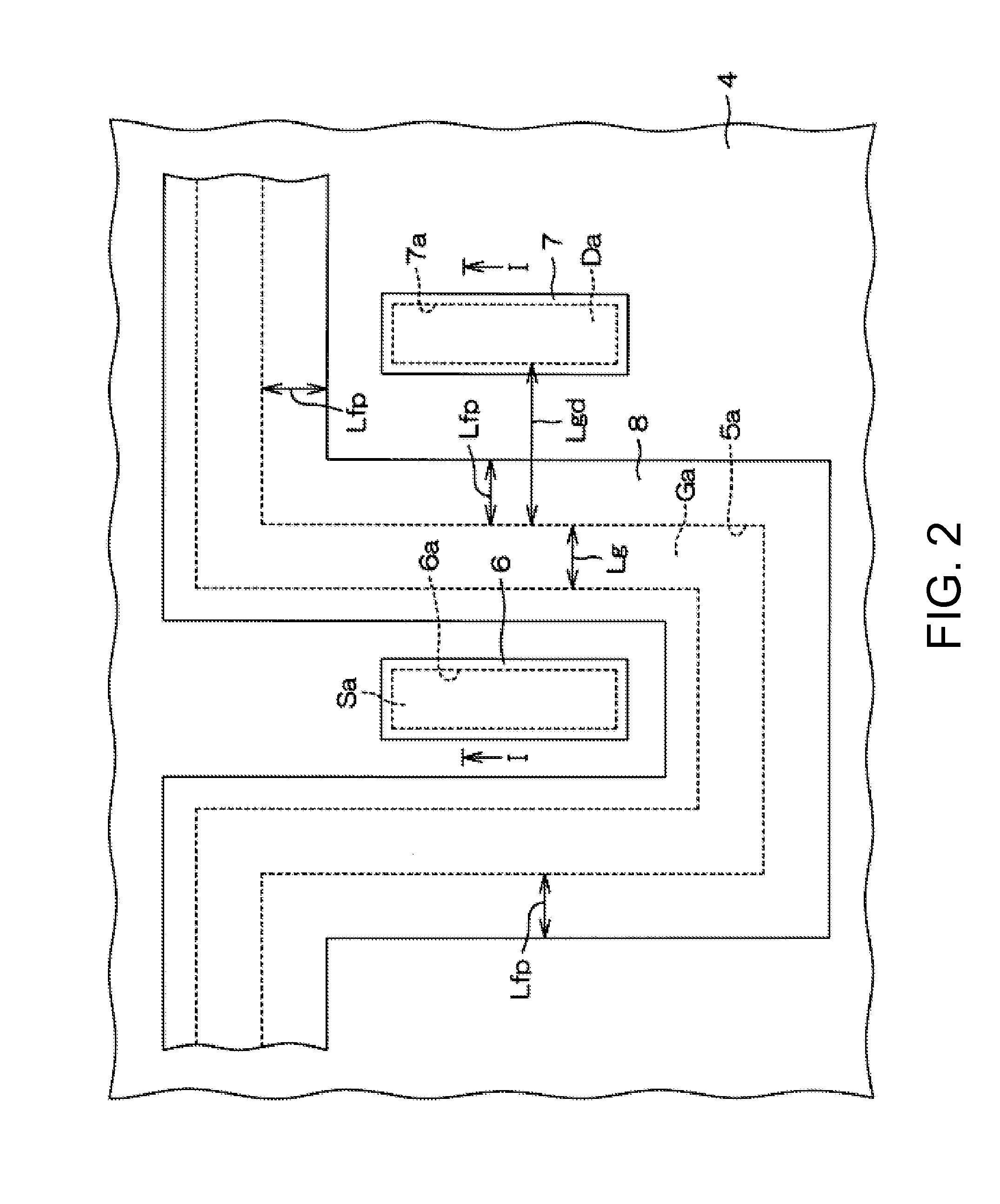
[0045]FIG. 1 is a cross-sectional view for describing a configuration of a nitride semiconductor device of the present invention. FIG. 2 is a plan view of the nitride semiconductor device. FIG. 1 shows a cross-section of FIG. 2 along the line I-I. The nitride semiconductor device includes a substrate 1 (a silicon substrate, for example), a buffer layer 2 formed on a surface of the substrate 1, an electron transport layer 3 formed on the buffer layer 2 by epitaxial growth, and an electron supply layer 4 formed on the electron transport layer 3 by epitaxial growth. The nitride semiconductor device further includes a gate insulating film 10 (not shown in FIG. 2) covering the surface of the electron supply layer 4, a passivation film 5 (not shown in FIG. 2) covering the gate insulating film 10, and a source electrode 6 and a drain electrode 7, which are ohmic electrodes in ohmic contact with the electron supply layer 4 through contact holes 6a and 7a formed in the gate insulating film ...

embodiment 2

[0075]FIG. 4 is a schematic cross-sectional view for describing a configuration of a nitride semiconductor device of the present invention. In FIG. 4, portions corresponding to the portions in FIG. 1 are assigned the same reference characters.

[0076]In the present embodiment, an electron supply layer 4 includes a second layer 42 as a cap layer formed on a first layer 41 that is made of AlGaN. A source electrode 6 and a drain electrode 7, which are ohmic electrodes, and a gate insulating film 10 are formed on the second layer 42, in contact therewith.

[0077]The second layer 42 is made of GaN, which is a nitride semiconductor of the same composition as an electron transport layer 3, and the thickness thereof is between 2 nm and 16 nm inclusive (more preferably 8 nm or less).

[0078]The second layer 42 functioning as a cap layer contributes to an improved surface morphology of the electron supply layer 4. In other words, on the surface of the electron transport layer 3 made of GaN, the fi...


PUM


Abstract

Provided are a nitride semiconductor device having an excellent boundary between a nitride semiconductor and a gate insulating film, resulting in improved device characteristics, and a manufacturing method therefor. The nitride semiconductor device includes: an electron transport layer made of a nitride semiconductor; an electron supply layer layered on the electron transport layer, the electron supply layer being made of a nitride semiconductor including Al and having an Al composition different from that of the electron transport layer; a source electrode and a drain electrode formed on the electron supply layer with a gap therebetween; a gate insulating film covering the surface of the electron supply layer between the source electrode and the drain electrode; a passivation film covering a surface of the gate insulating film and having an opening between the source electrode and the drain electrode; and a gate electrode having a main gate body in the opening facing the electron supply layer through the gate insulating film.

Description

[0001]This application claims the benefit of Japanese Application No. 2012-118826, filed in Japan on May 24, 2012, which is hereby incorporated by reference in its entirety.BACKGROUND OF THE INVENTION[0002]1. Field of the Invention[0003]The present invention relates to a semiconductor device made of a group III nitride semiconductor (sometimes referred to simply as a “nitride semiconductor” below) and a manufacturing method therefor.[0004]2. Description of Related Art[0005]A group III nitride semiconductor is a semiconductor that uses nitrogen as the group V element in a group III-V semiconductor. Aluminum nitride (AlN), gallium nitride (GaN), and indium nitride (InN) are representative examples thereof. In general, it is possible to express this as AlXInYGa1-X-YN (0≦X≦1, 0≦Y≦1, 0<X+Y<1).[0006]A MISFET (metal-insulator-semiconductor field effect transistor) using such a nitride semiconductor is proposed. Patent Document 1 discloses one example of such a MISFET. The MISFET disc...

Claims


Application Information

Patent Timeline
IPC IPC(8): H01L29/78H01L29/66
CPCH01L29/78H01L29/66477H01L29/432H01L29/513H01L29/66462H01L29/7786H01L29/2003H01L29/517H01L29/518
Inventor AKUTSU, MINORUFUJIWARA, TETSUYA
Owner ROHM CO LTD
Why Eureka
Try Eureka