

System and method for photonically assisted analog to digital signal conversion
- Summary
- Abstract
- Description
- Claims
- Application Information
AI Technical Summary
Benefits of technology
Problems solved by technology
Method used
Image

Examples
Embodiment Construction
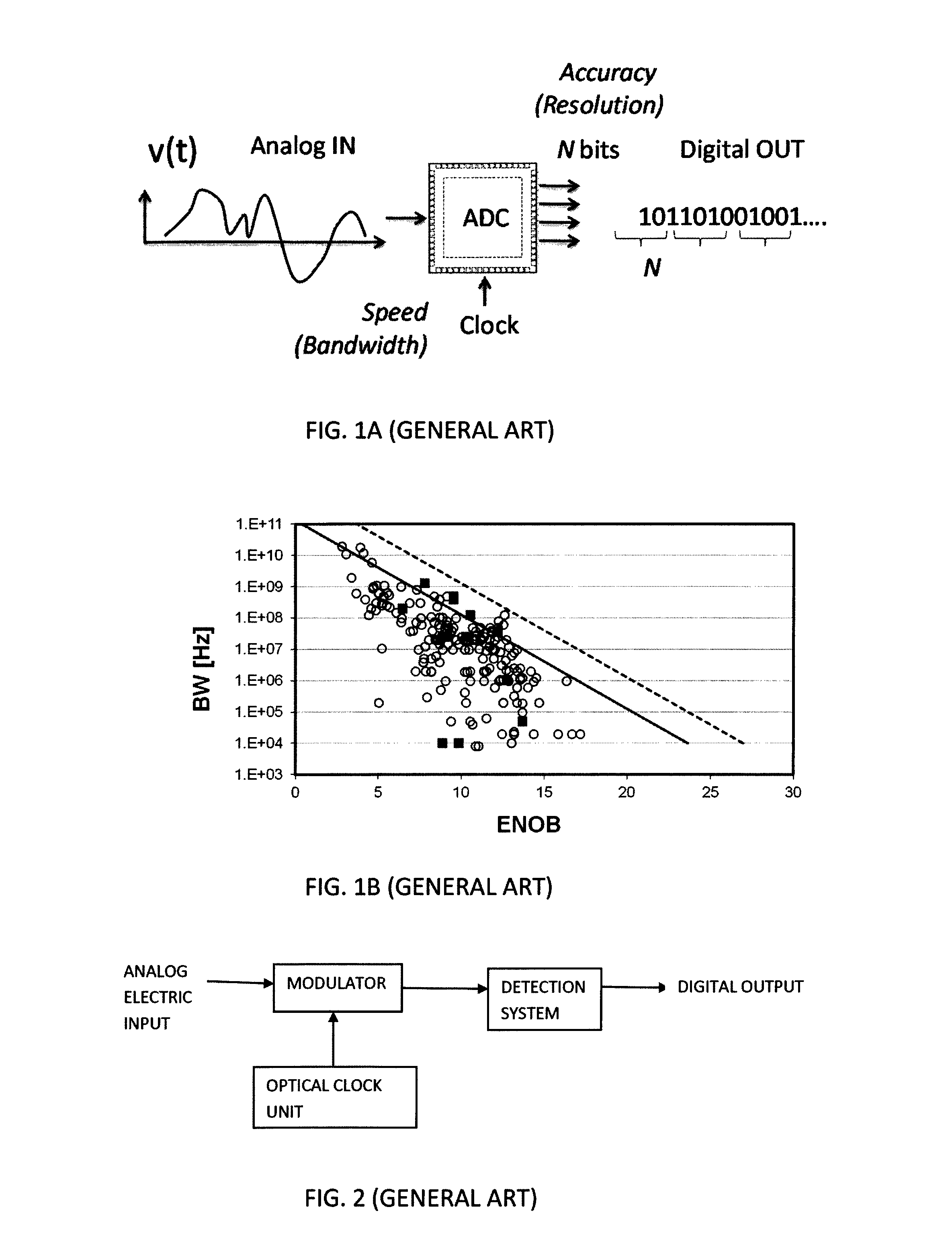
[0062]FIG. 1A schematically illustrates the principles of electronic ADC technology, and FIG. 1B illustrates the state of the art ADC technology at the time of submission. FIG. 2 shows a typical photonic ADC system.
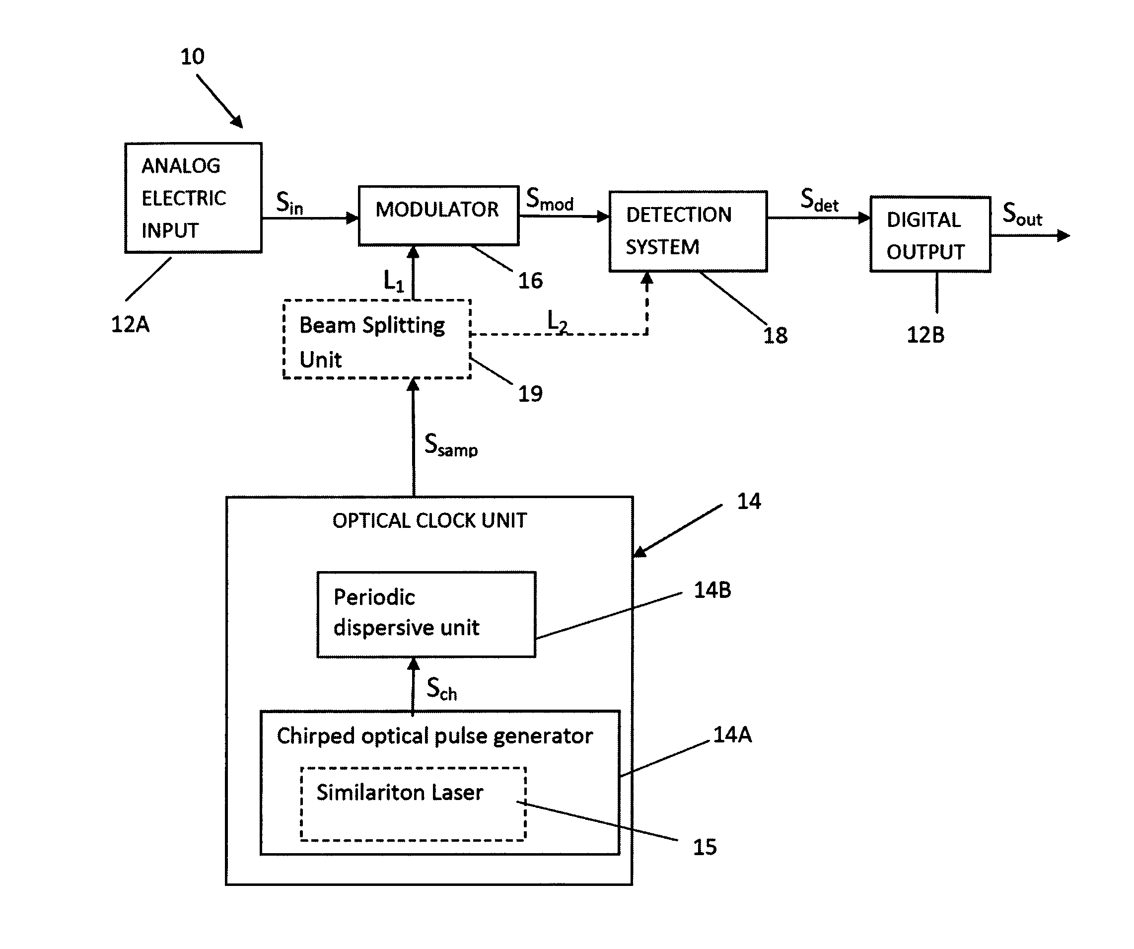
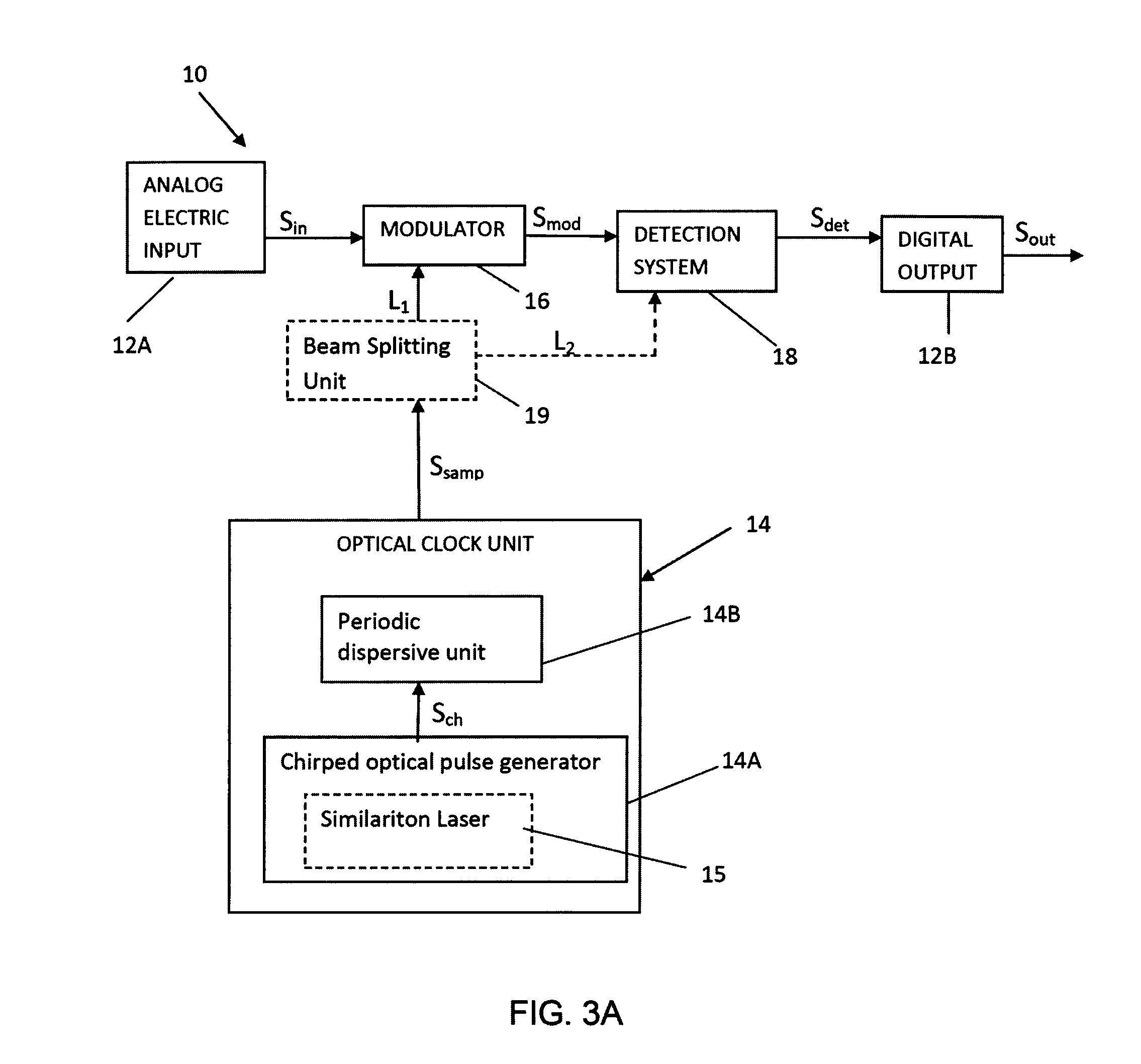
[0063]Reference is made to FIGS. 3A to 3D showing four examples, respectively, of a photonically-assisted ADC system of the present invention. To facilitate understanding, the same reference numbers are used for identifying those components which are common in all the examples of the invention.
[0064]A system of the present invention, generally designated 10, is configured as internally-photonic structure but with electronic input / output interfaces, and includes the following main functional components: input and output ports 12A and 12B for inputting analog electric input Sin and outputting digital electric output Sout; an optical sampling signal generator (optical clock unit) 14, modulator 16 and detection system 18. Optical clock unit 14 is configured for producing a sa...
PUM
 Abstract
Description
Claims
Application Information