

Integrated inertial sensor and pressure sensor, and forming method therefor
a technology of inertial sensor and pressure sensor, applied in the field of semiconductors, can solve the problems of no integrated sensor product on the market now, high cost, complicated overall process, etc., and achieve the effect of large size and high cos
- Summary
- Abstract
- Description
- Claims
- Application Information
AI Technical Summary
Benefits of technology
Problems solved by technology
Method used
Image

Examples
first embodiment
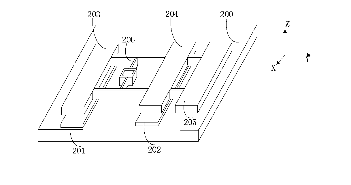
[0162]By the above processes, the integrated inertial sensor and pressure sensor according to the invention is formed. In FIG. 16, the dashed box 10 indicates the formed pressure sensor, and the dashed box 20 indicates the formed inertial sensor. Specifically, the integrated inertial sensor and pressure sensor includes the movable electrode 407 of the inertial sensor and the fixed electrode 410 of the pressure sensor; the second substrate 501′ and the third substrate 701. The movable electrode 407 of the inertial sensor and the fixed electrode 410 of the pressure sensor are arranged between the second substrate 501′ and the third substrate 701. The movable electrode 407 of the inertial sensor 20 is formed by using the first substrate. The fixed electrode 410 of the pressure sensor is formed by using the first substrate. The first substrate is monocrystalline semiconductor material. The first substrate includes a first surface and a second surface. The first substrate includes a firs...
second embodiment
[0166]the integrated inertial sensor and pressure sensor is further provided according to the present invention, and referred to in FIG. 17. The structure shown in FIG. 17 differs from the structure shown in FIG. 16 in that the coupling layer between the first substrate and the second substrate is exposed through the pressure port opening 502, and the second conductive layer and the coupling layer in the second region II together serve as the sensitive film of the pressure sensor. In this embodiment, the coupling layer is an insulating layer, and can protect the second conductive layer.
[0167]The sensitive film may also be formed of other conductive materials and insulating layers in combination, and may have other variations in the following embodiments. Further, the sensitive film may include more material layers, as long as the sensitive film includes one conductive layer and can be deformed under the action of external force.
[0168]The method for forming the integrated inertial se...
third embodiment
[0169]the integrated inertial sensor and pressure sensor is further provided according to the invention, and FIG. 18 is referred to. The structure shown in FIG. 18 differs from the structure shown in FIG. 16 in that the second conductive layer for forming the first electrical shielding layer of the inertial sensor is exposed through the pressure port opening 502, and no additional movable electrode of the pressure sensor is formed, i.e., the exposed second conductive layer serves not only as the sensitive film of the pressure sensor but also the movable electrode of the pressure sensor. All the conductive layers between the fixed electrode and the sensitive film of the pressure sensor are removed, and a third air cavity is formed. The third air cavity, the through hole in the fixed electrode of the pressure sensor, and the seventh air cavity are in communication with one another. The sensitive film of the pressure sensor and the fixed electrode of the pressure sensor form two parall...
PUM
 Abstract
Description
Claims
Application Information