

Metal nanowire networks and transparent conductive material
a technology of metal nanowires and transparent conductive materials, applied in the direction of resistive material coating, metallic pattern materials, metallic material coating processes, etc., can solve the problems of low cost, relative slowness, and easy cracking of flexible substrates
- Summary
- Abstract
- Description
- Claims
- Application Information
AI Technical Summary
Benefits of technology
Problems solved by technology
Method used
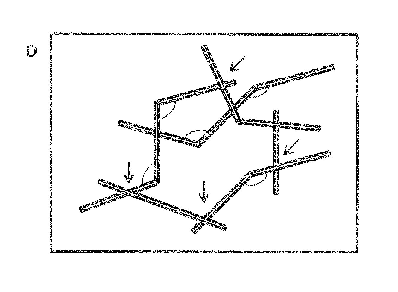
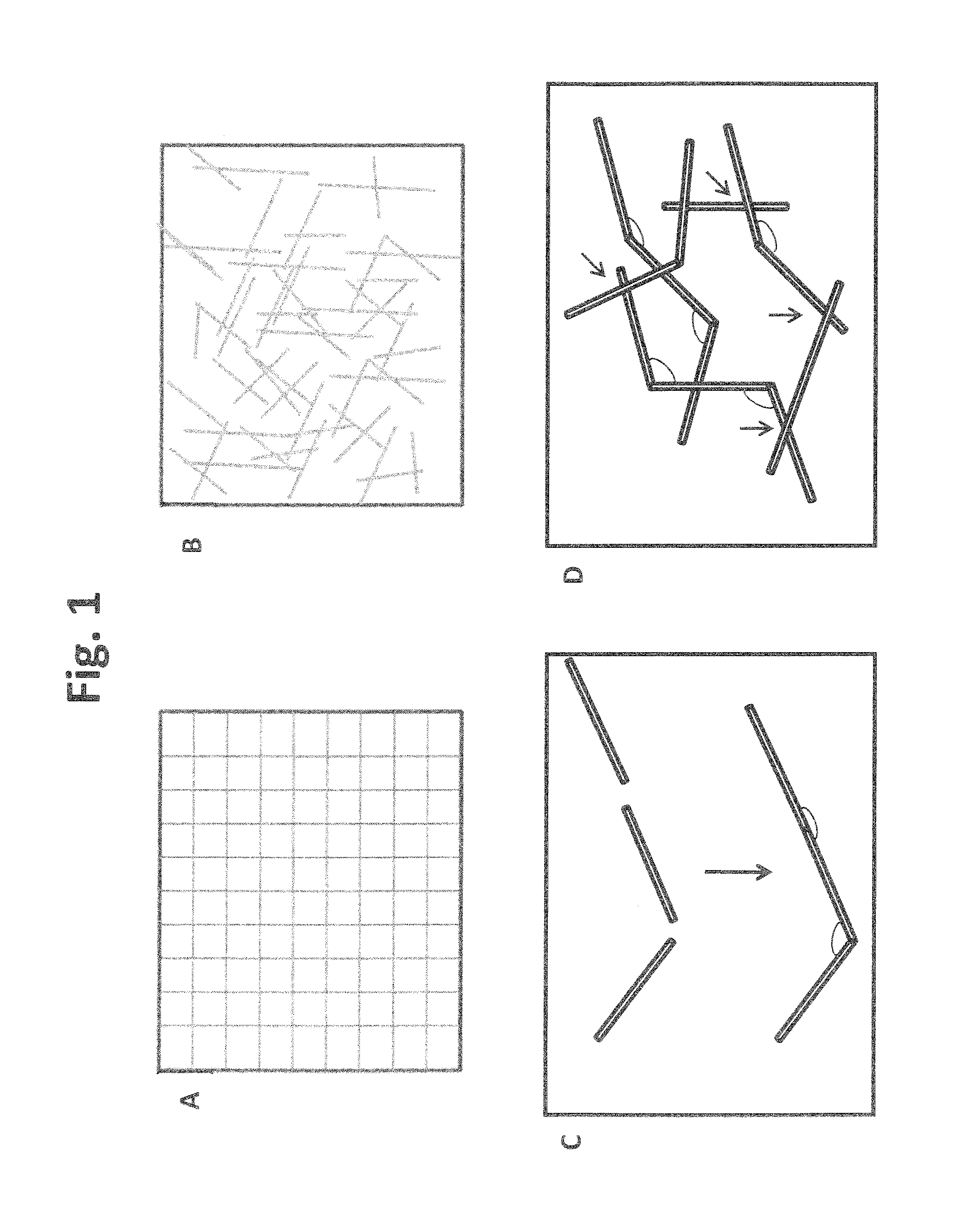
Image

Examples
example 1
Fabrication of Transparent Conductive Material Using HCl Vapor Treatment
[0051]This example demonstrates the ability to use a vapor based fusing agent to chemically drive the fusing of silver nanowires to dramatically improve the electrical conductivity.
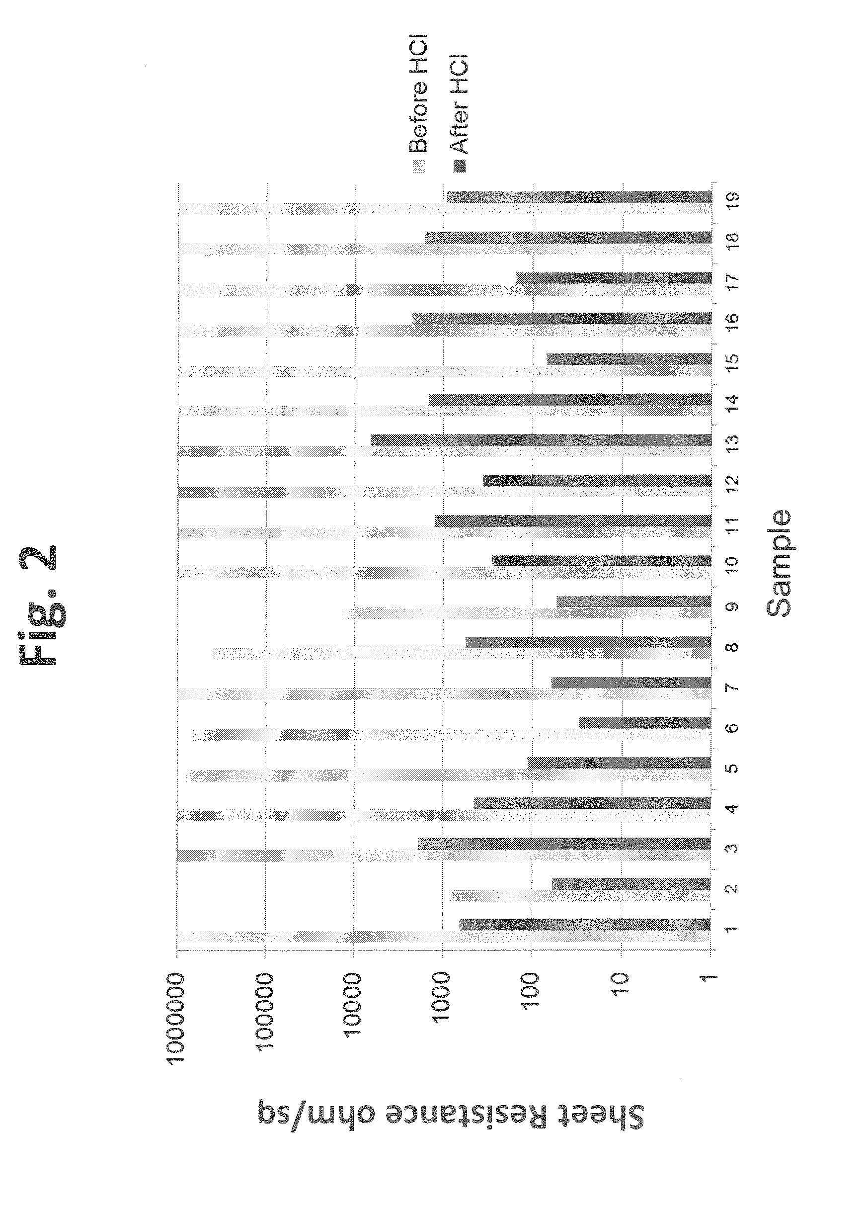
[0052]Commercially available silver nanowires (AgNWs) were dispersed in alcohols e.g. ethanol or isopropanol to form an AgNWs dispersion. The AgNWs dispersions were typically in the 0.1-1.0% wt range. The dispersion was then deposited on glass or polyethylene terephthalate (PET) surfaces as an AgNWs film using a spray coating or a hand-drawn rod approach. The AgNWs film was then exposed briefly to HCl vapour as a fusing agent. Specifically, the AgNWs film was exposed to HCl vapour from a concentrated HCl solution at room temperature for about 10 seconds. AgNWs from two different vendors were used. The sheet resistance and transparency of the AgNWs film before and after the treatment with HCl vapour were measured and recorded. The data...
example 2
Observation of the Fusing of the Silver Nanowires
[0055]This example provides evidence of nanowire physical fusing as a result of contact with chemical fusing agents.
[0056]The dramatic conductivity improvement observed in Example 1 can be attributed to the fusing of some of the silver nanowires with adjacent silver nanowires. Scanning electron micrographs (SEM) of the silver nanowires before treatment were obtained and are shown in FIG. 5. As shown in FIG. 5, some of the ends (indicated by the circles) of the silver nanowires appear to touch each other, but the ends apparently do not appear to be fused together. Additionally, polyvinylpyrrolidone (PVP) coating (indicated by arrows in the figure) can be seen to be present around the rods. As a comparison, the silver nanowires shown in FIG. 5 were heated at 100° C. for 10 minutes. No appreciable conductivity change has been observed after the heating. SEM micrographs of the silver nanowires after the heat treatment were obtained and ar...
example 3
Fabrication of Transparent Conductive Material Using Halide Solution Treatment
[0057]This example demonstrated the reduction in electrical resistance through the treatment of the networks with solutions containing halide anions.
[0058]Specifically, 50 mM solutions of AgF or NaCl in ethanol were used to treat the AgNWs films. When the fusing agent solution is used, the AgNWs film was submerged or covered with the fusing agent solution for about 10 to about 30 seconds, or dilute solutions of AgF or NaCl were spray coated (from ethanol) onto the AgNW. The AgNWs were then allowed to dry. The sheet resistance of the AgNWs film before and after the treatment with the halide solutions were measured and the results are shown in FIG. 8. As shown in FIG. 8 dramatic conductivity improvement is also observed of the AgNWs films treated with halide solutions, with AgF treated samples showing even more pronounced improvement compared to the NaCl treated samples. In general, the transmission of light...
PUM
| Property | Measurement | Unit |
|---|---|---|
| sheet resistance | aaaaa | aaaaa |
| transparency | aaaaa | aaaaa |
| sheet resistance | aaaaa | aaaaa |
Abstract
Description
Claims
Application Information