Method for manufacturing a component having an electrical through-connection

Active Publication Date: 2013-12-26
ROBERT BOSCH GMBH
View PDF2 Cites 14 Cited by
  • Summary
  • Abstract
  • Description
  • Claims
  • Application Information

AI Technical Summary

Benefits of technology

[0009]An object of the present invention, therefore, is to provide a via-middle approach for producing an electrical through-connection which a

Problems solved by technology

However, these standard processes are not suited for metal plating a through-connection in the cap of an already capped sensor wafer, since the bonding layer may be attacked by the electroplating baths used, and which may flow through

Method used


Image

  • Method for manufacturing a component having an electrical through-connection
  • Method for manufacturing a component having an electrical through-connection
  • Method for manufacturing a component having an electrical through-connection

Examples


Embodiment Construction

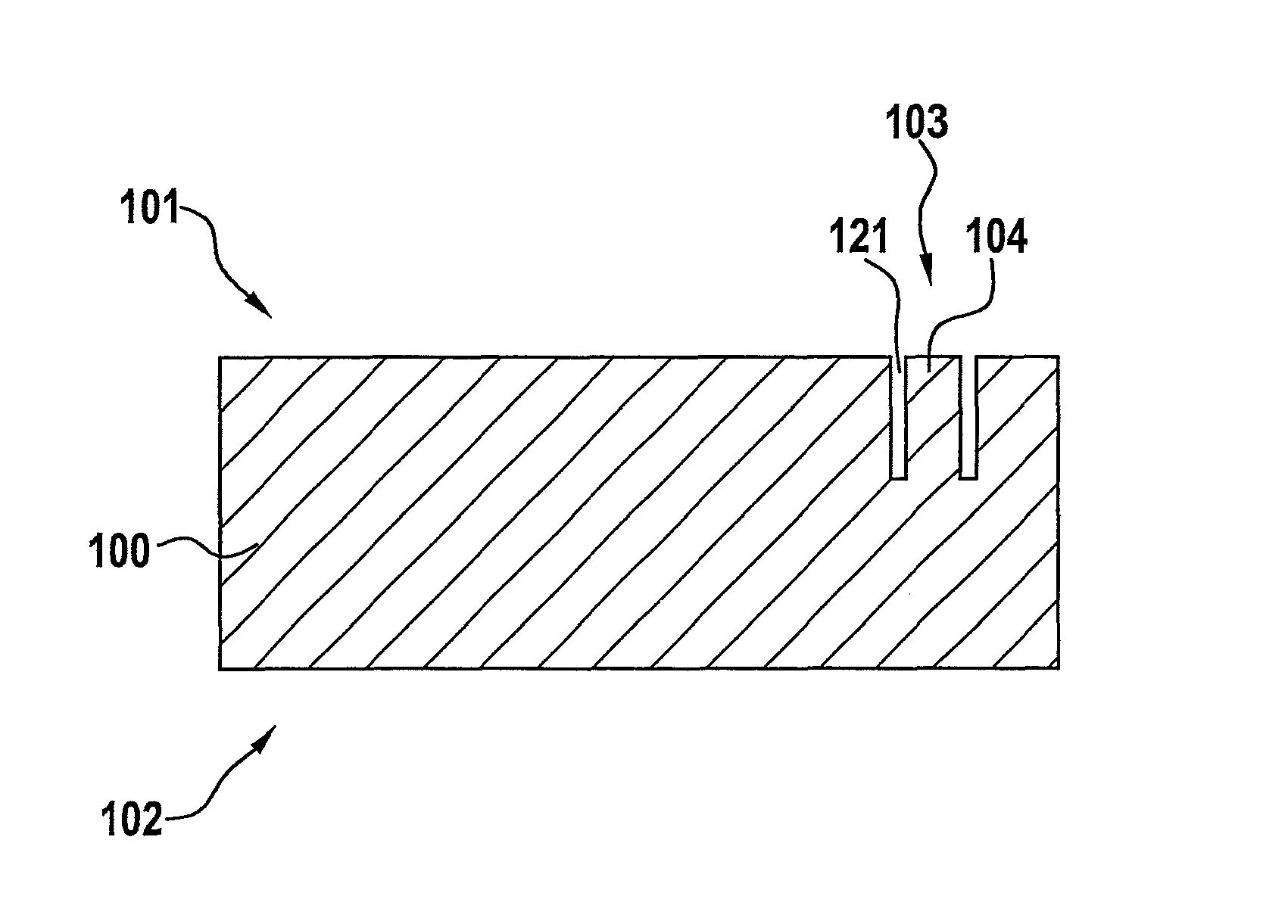
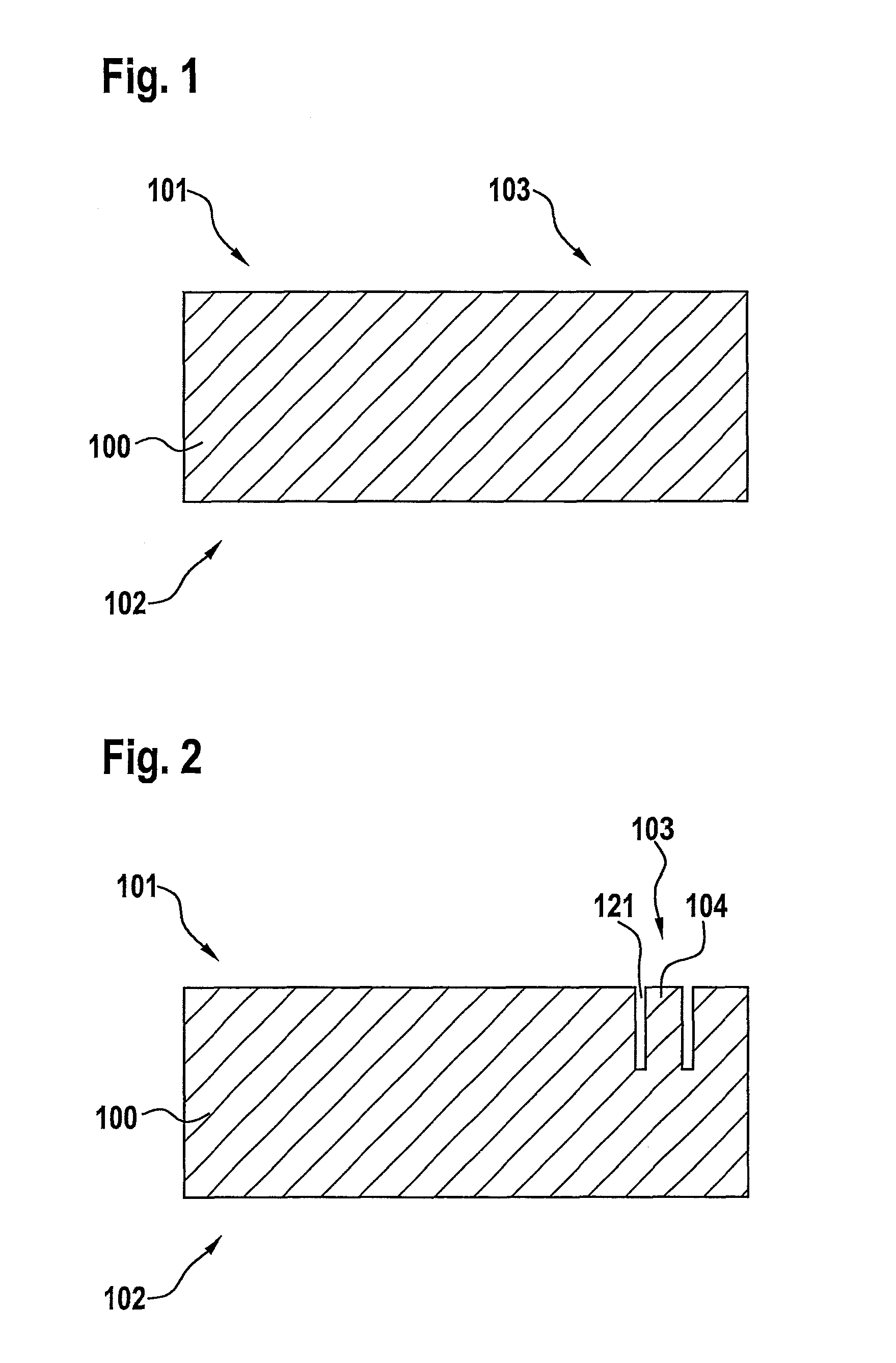
[0038]The method according to the present invention is explained in greater detail below as an example, with reference to the manufacture of a microelectromechanical component such as a microelectromechanical motion sensor or yaw rate sensor, having at least one microelectromechanical functional structure. At least one through-connection is produced in a semiconductor substrate which is used as a cap wafer for the microelectromechanical functional structure situated on the functional substrate. The starting point is semiconductor substrate 100, for example in the form of a silicon wafer. FIG. 1 shows semiconductor substrate 100, having a front side 101 and a back side 102 opposite from the front side.

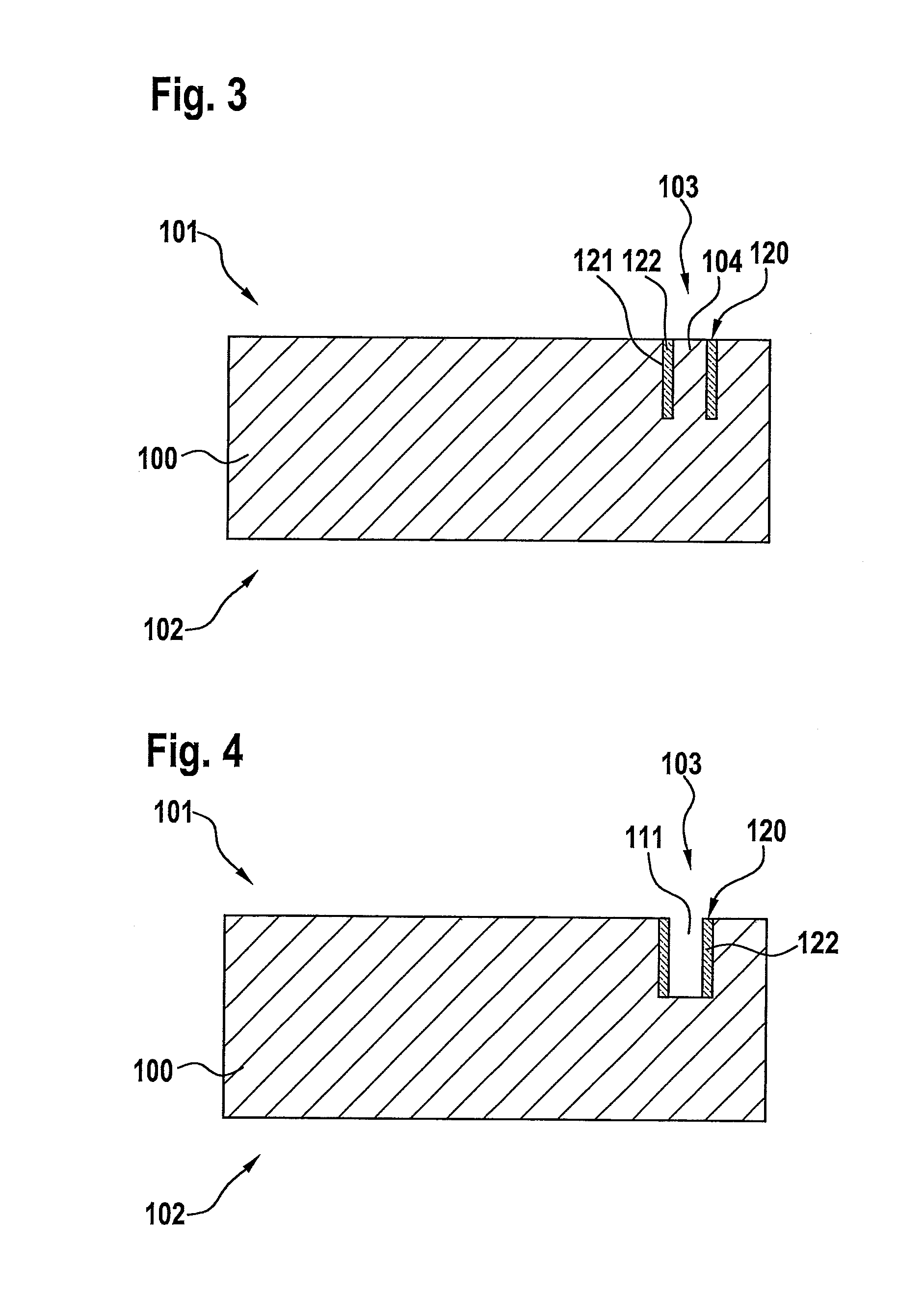
[0039]An insulating trench 121 which annularly surrounds a contact area 103 is initially produced in semiconductor substrate 100.

[0040]This is preferably carried out with the aid of a customary trench process, in which a mask layer (TEOS oxide or aluminum, for example) is initially appl...


PUM

PropertyMeasurementUnit
Structureaaaaaaaaaa
Metallic bondaaaaaaaaaa
Semiconductor propertiesaaaaaaaaaa

Abstract

A method for manufacturing a component having an electrical through-connection includes: providing a semiconductor substrate having a front side and a back side opposite from the front side; producing, on the front side of the semiconductor substrate, an insulating trench which annularly surrounds a contact area; introducing an insulating material into the insulating trench; producing a contact hole on the front side of the semiconductor substrate by removing the semiconductor material surrounded by the insulating trench in the contact area; and depositing a metallic material in the contact hole.

Description

BACKGROUND OF THE INVENTION[0001]1. Field of the Invention[0002]The present invention relates to a method for manufacturing a component, in particular a microelectromechanical component, having a through-connection.[0003]2. Description of the Related Art[0004]The development of increasingly smaller packets of micro-electromechanical components (MEMS, microelectromechanical system) requires, among other things, stacking and through contacting of individual elements such as a sensor, a sensor cap, and an evaluation circuit (ASIC). Arranging the elements one on top of the other is referred to as MEMS 3D integration. The so-called through silicon vias (TSV) are one option for a through-connection in microelectromechanical components built up on silicon substrates. Such TSV structures must meet a number of criteria concerning their electrical resistance and mechanical stability. In the stacking of various microcomponents such as sensors and ASICs, it is particularly important, among othe...

Claims


Application Information

Patent Timeline
IPC IPC(8): B81C1/00B81B3/00
CPCB81C1/00134B81B3/0018B81B7/007B81B2207/095
Inventor REINMUTH, JOCHENFREY, JENSBERGMANN, YVONNE
Owner ROBERT BOSCH GMBH
Why Eureka
Try Eureka