Semiconductor device and method for manufacturing semiconductor device

a semiconductor and semiconductor technology, applied in the direction of semiconductor devices, electrical devices, transistors, etc., can solve the problems of different electrical characteristics of transistors, and achieve the effects of improving the on-state characteristics of transistors including oxide semiconductor films, improving reliability, and improving stable electric characteristics

Active Publication Date: 2014-01-02
SEMICON ENERGY LAB CO LTD
View PDF3 Cites 58 Cited by
  • Summary
  • Abstract
  • Description
  • Claims
  • Application Information

AI Technical Summary

Benefits of technology

[0025]According to one embodiment of the present invention, on-state characteristics of a transistor including an oxide semiconductor film can be improved. Alternatively, stable electric characterist...

Problems solved by technology

In a transistor including an oxide semiconductor film, unintended impurities such as hydrogen or moisture enter the ...

Method used


Image

  • Semiconductor device and method for manufacturing semiconductor device
  • Semiconductor device and method for manufacturing semiconductor device
  • Semiconductor device and method for manufacturing semiconductor device

Examples


embodiment 1

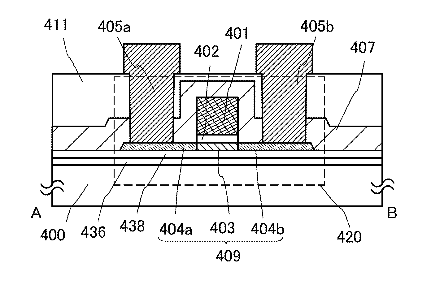
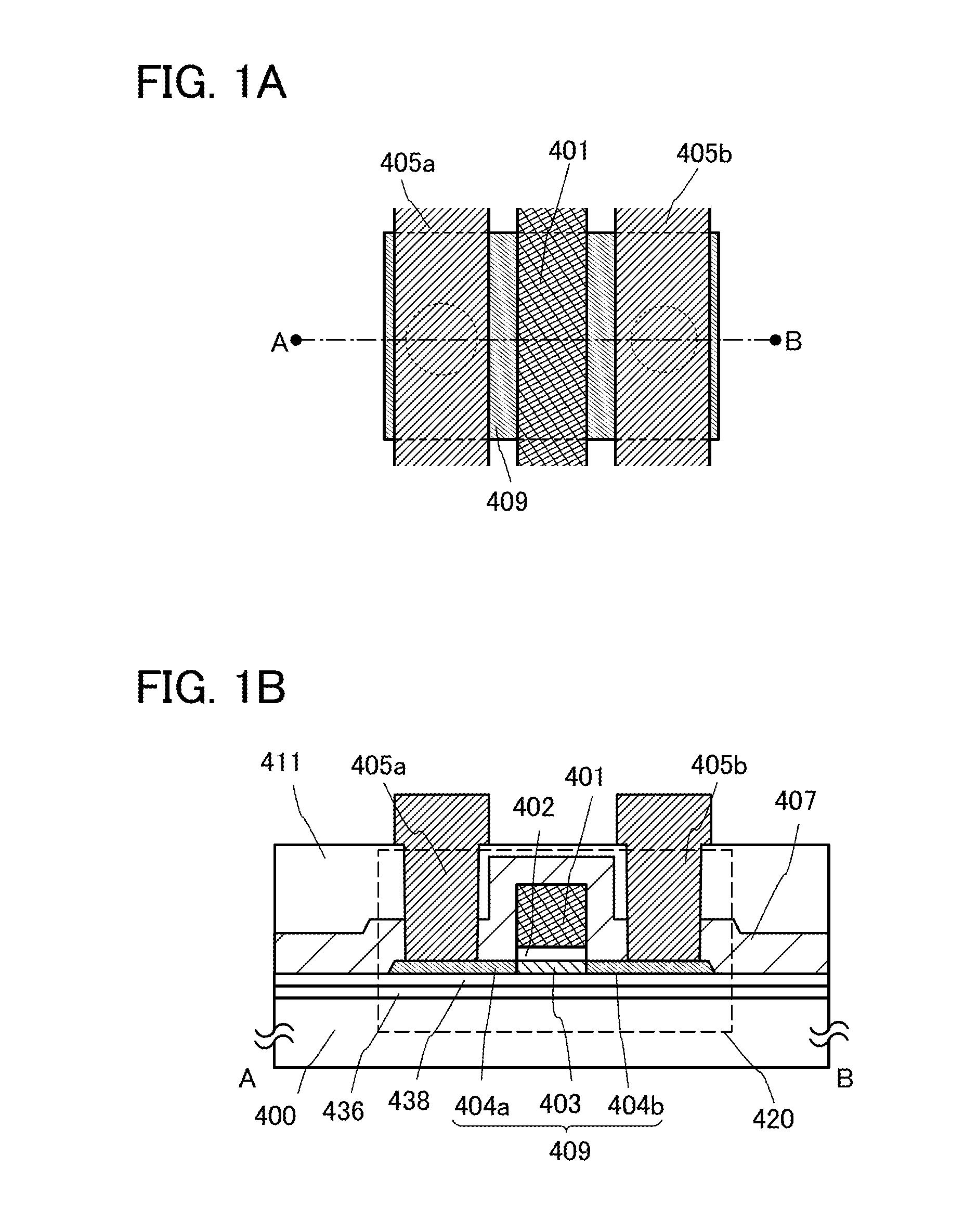
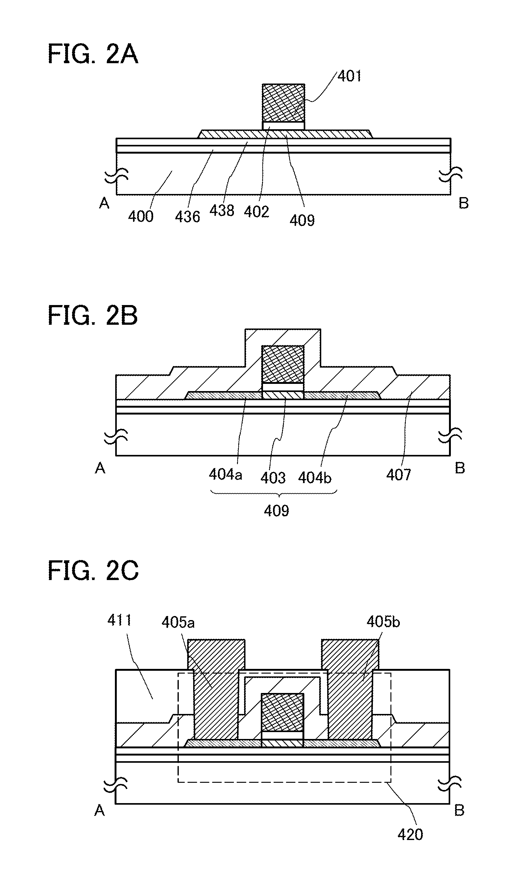
[0052]In this embodiment, a semiconductor device according to one embodiment of the present invention is described in detail with reference to drawings. FIGS. 1A and 1B are respectively a top view and a cross-sectional view of a transistor 420 that is a semiconductor device according to one embodiment of the present invention. FIG. 1A is the top view of the transistor 420, and FIG. 1B is the cross-sectional view taken along dashed-dotted line A-B in FIG. 1A.

[0053]The transistor 420 in FIGS. 1A and 1B includes the following: a base insulating film 436 over a substrate 400; an oxide semiconductor film 409 which is over the base insulating film 436 and includes a channel formation region 403, a low-resistance region 404a, and a low-resistance region 404b; a gate insulating film 402 and a gate electrode layer 401 which are over the channel formation region 403; a silicon nitride film 407 over the oxide semiconductor film 409, the gate insulating film 402, and the gate electrode layer 40...

embodiment 2

[0172]In this embodiment, transistors according to one embodiment of the present invention which are different from those of Embodiment 1 are described. Note that, in this embodiment, portions that are similar to the portions in Embodiment 1 are denoted by the same reference numerals, and detailed description thereof is omitted.

[0173]FIGS. 4A and 4B illustrate a transistor 520 according to one embodiment of the present invention. FIG. 4A is a top view of the transistor 520 and FIG. 4B is a cross-sectional view taken along dashed-dotted line C-D in FIG. 4A.

[0174]The transistor 520 includes the following: the base insulating film 436 and the base insulating film 438 over the substrate 400; an oxide semiconductor film 509 over the base insulating film 438; the gate insulating film 402 over the oxide semiconductor film 509; the gate electrode layer 401 over the gate insulating film 402; a sidewall insulating film 413a and a sidewall insulating film 413b which are in contact with side su...

embodiment 3

[0208]In this embodiment, an example of a semiconductor device including any of the transistors described in Embodiments 1 and 2 is described with reference to FIG. 7 and FIGS. 8A and 8B.

[0209]FIG. 7 is a cross-sectional view of part of a semiconductor device described in this embodiment. The cross-sectional view illustrated in FIG. 7 is an example, and the structure of the semiconductor device described in this embodiment is not limited thereto.

[0210]The semiconductor device illustrated in FIG. 7 includes a transistor 160 including a first semiconductor material in a lower portion, and a transistor 162 including a second semiconductor material in an upper portion. The transistor 162 can have a structure similar to that of any of the transistors described in Embodiments 1 and 2. Here, as the transistor 162, the transistor described in Embodiment 1 is used.

[0211]Here, the first semiconductor material and the second semiconductor material are preferably materials having different band...


PUM


Abstract

In a top-gate transistor in which an oxide semiconductor film, a gate insulating film, a gate electrode layer, and a silicon nitride film are stacked in this order and the oxide semiconductor film includes a channel formation region, nitrogen is added to regions of part of the oxide semiconductor film and the regions become low-resistance regions by forming a silicon nitride film over and in contact with the oxide semiconductor film. A source and drain electrode layers are in contact with the low-resistance regions. A region of the oxide semiconductor film, which does not contact the silicon nitride film (that is, a region overlapping with the gate insulating film and the gate electrode layer) becomes the channel formation region.

Description

BACKGROUND OF THE INVENTION[0001]1. Field of the Invention[0002]One embodiment of the present invention relates to a semiconductor device and a method for manufacturing the semiconductor device.[0003]In this specification, the semiconductor device refers to all the devices that operate by utilizing semiconductor characteristics. For example, electro-optical devices, semiconductor circuits, and electronic devices are all included in the category of the semiconductor device.[0004]2. Description of the Related Art[0005]Attention has been focused on a technique for forming a transistor using a semiconductor thin film formed over a substrate having an insulating surface (also referred to as a thin film transistor (TFT)). The transistor is applied to a wide range of electronic devices such as an integrated circuit (IC) or an image display device (display device). A silicon film is widely known as the semiconductor thin film applicable to the transistor. As another film, an oxide semicondu...

Claims


Application Information

Patent Timeline
IPC IPC(8): H01L29/786H01L29/66
CPCH01L29/78693H01L29/66969H01L29/78618H01L29/78621H01L29/7869H01L29/66742H01L29/78606H01L21/0217H01L21/441
Inventor YAMAZAKI, SHUNPEIOKAZAKI, KENICHIKOEZUKA, JUNICHISASAKI, TOSHINARI
Owner SEMICON ENERGY LAB CO LTD
Why Eureka
Try Eureka