High efficiency solar cells fabricated by inexpensive pecvd

a solar cell, low-cost technology, applied in the field of photovoltaic devices and methods for fabrication, can solve the problems of low productivity, achieve the effects of improving overall performance, high deposition rate, and enhancing chemical vapor deposition

Active Publication Date: 2014-01-02
GLOBALFOUNDRIES US INC
View PDF29 Cites 17 Cited by
  • Summary
  • Abstract
  • Description
  • Claims
  • Application Information

AI Technical Summary

Benefits of technology

[0005]A method for forming a photovoltaic device includes depositing one or more layers of a photovoltaic stack on a substrate by employing a high deposition rate plasma enhanced chemical vapor deposition (HDR PECVD) process. Contacts are formed on the photovoltaic stack to provide a photovoltaic cell. Annealing is performed on the photovoltaic cell at a temperature and duration configured to improve overall performance.

Problems solved by technology

These processes result in low productivity and stand in the way of the impetus to further solar power as a long term energy solution.

Method used


Image

  • High efficiency solar cells fabricated by inexpensive pecvd
  • High efficiency solar cells fabricated by inexpensive pecvd
  • High efficiency solar cells fabricated by inexpensive pecvd

Examples


Embodiment Construction

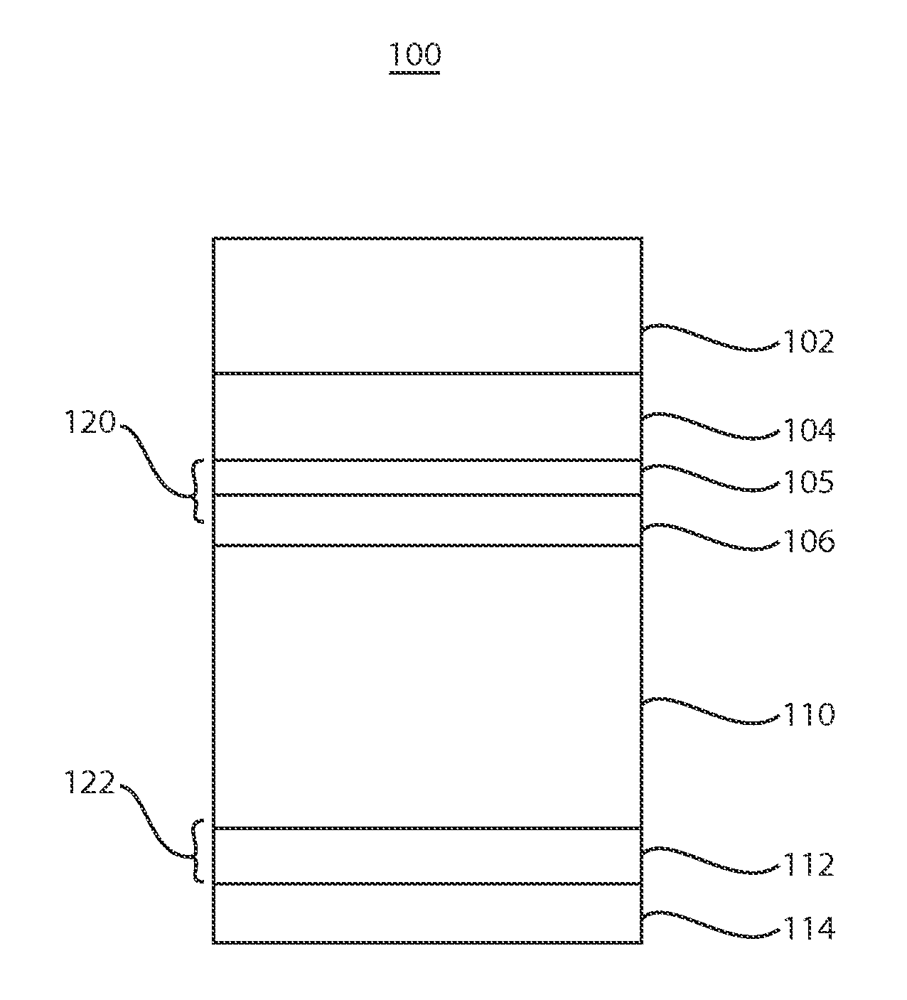
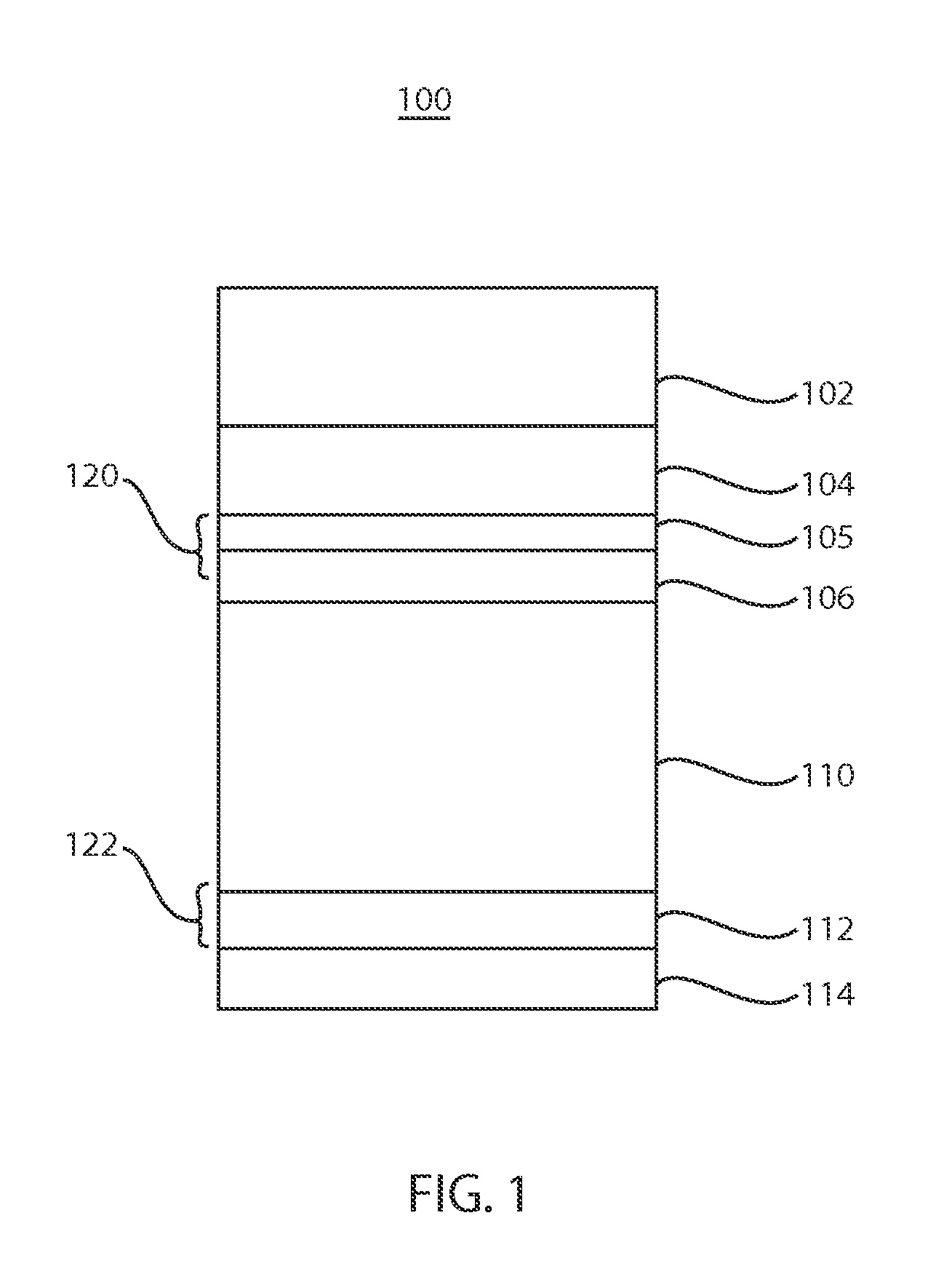
[0016]In accordance with the present principles, methods and devices are presented that provide improved efficiency to photovoltaic cells fabricated with high deposition rate and high throughput processes. Layers for semiconductor devices are often deposited using low deposition energies. Low deposition energies are favored by manufacturing since the low energy permits high quality a-Si:H layer deposition and less energy usage. Designers also prefer low deposition energies since the low energies create plasma with less energy bombardment on a surface resulting in less damage to existing structures on semiconductor devices. In thin film Si solar cell applications, high deposition energies are desired for depositing a p+ layer since the higher energies increase the likelihood that a microcrystalline phase will form. The microcrystalline phase can reduce barrier heights between the p+ layer and an electrode (e.g., formed from a transparent conductive oxide (TCO)).

[0017]For example, pho...


PUM


Abstract

A method for forming a photovoltaic device includes depositing one or more layers of a photovoltaic stack on a substrate by employing a high deposition rate plasma enhanced chemical vapor deposition (HDR PECVD) process. Contacts are formed on the photovoltaic stack to provide a photovoltaic cell. Annealing is performed on the photovoltaic cell at a temperature and duration configured to improve overall performance.

Description

BACKGROUND[0001]1. Technical Field[0002]The present invention relates to photovoltaic devices and methods for fabrication, and more particularly to systems, devices and fabrication methods that improve efficiency for devices fabricated with inexpensive deposition tools.[0003]2. Description of the Related Art[0004]With the push for more efficient and cheaper solar energy, higher throughput and lower expense tools are needed for producing solar panels. Conventional solar panel production typically relies of plasma enhanced chemical vapor deposition tools that require ultra high vacuum and low deposition rates (e.g., 1 angstrom / sec) in order to achieve sufficient quality. Such processes are marked by low plasma power (to reduce cost and protect the device being fabricated) and low gas pressure. These processes result in low productivity and stand in the way of the impetus to further solar power as a long term energy solution.SUMMARY[0005]A method for forming a photovoltaic device inclu...

Claims


Application Information

Patent Timeline
Patent Type & Authority Applications(United States)
IPC IPC(8): H01L31/18
CPCH01L31/022425H01L31/03921H01L31/075H01L31/1864Y02E10/548Y02P70/50H01L21/00H01L31/18
Inventor FOGEL, KEITH E.HONG, AUGUSTIN J.KIM, JEEHWANSADANA, DEVENDRA K.
Owner GLOBALFOUNDRIES US INC
Why Eureka
Try Eureka