Organic solar cell
a solar cell and organic technology, applied in the field of organic solar cells, can solve the problems of unfavorable absorbing of light of relatively wide wavelength regions, deteriorating performance of tandem organic solar cells, and low output current, so as to prevent or reduce performance degradation by excessive charges
- Summary
- Abstract
- Description
- Claims
- Application Information
AI Technical Summary
Benefits of technology
Problems solved by technology
Method used
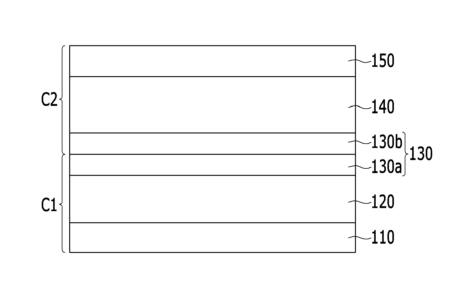
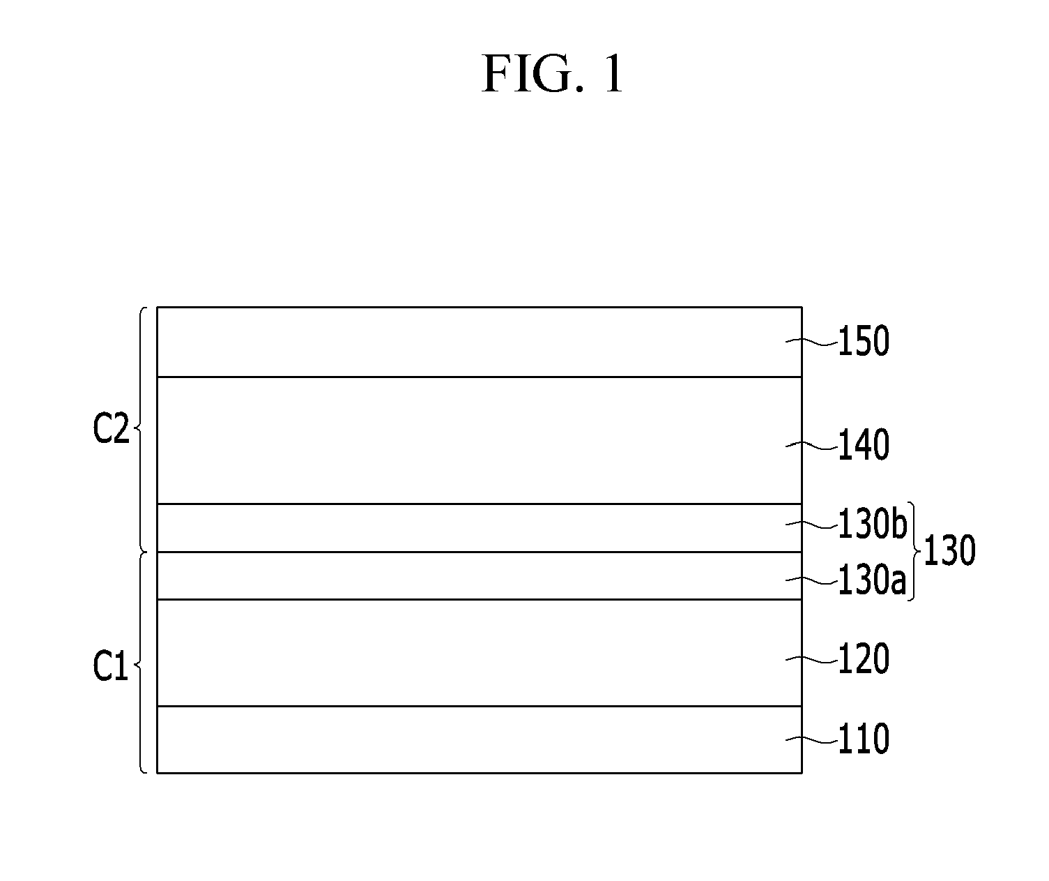
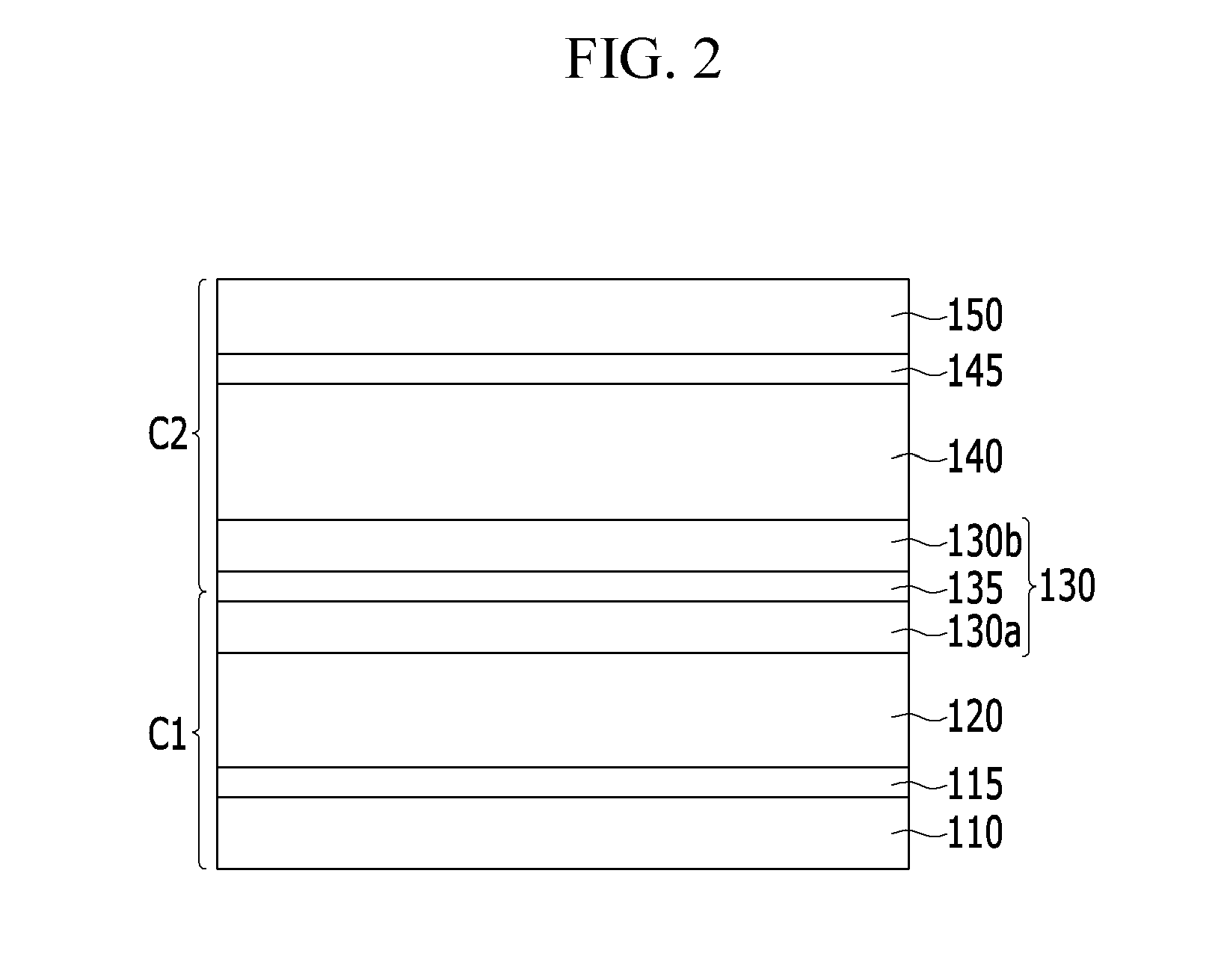
Image

Examples
example 1
[0110]A 180 nm thick ITO anode is formed on a 1 mm-thick transparent glass substrate by a sputtering method.
[0111]An active layer is formed on the ITO anode by applying a solution prepared by dissolving an electron donor (Mn=25,000) represented by the following Chemical Formula A and a PC60BM / PC70BM electron acceptor in chlorobenzene:1,8-diiodooctane (97:3, v / v).
[0112]Herein, the electron donor represented by Chemical Formula A is mixed with PC60BM and PC70BM in a weight ratio of 10:7.5:7.5 (w / w).
[0113]A 100 nm thick aluminum (Al) cathode is formed on the active layer, manufacturing a solar cell.
example 2-1
[0129]A 180 nm-thick ITO anode is formed on a 1 mm-thick transparent glass substrate by a sputtering method.
[0130]A 30 nm-thick lower auxiliary layer is formed on the ITO anode by spin-coating PEDOT:PSS.
[0131]An 85 nm-thick active layer is formed on the lower auxiliary layer by applying a solution prepared by dissolving an electron donor (Mn=34,000) represented by the following Chemical Formula B and a PC60BM / PC70BM electron acceptor in a ratio of 1:2 (w / w) in chlorobenzene:1,8-diiodooctane (97:3, v / v).
[0132]Herein, the electron acceptor compounds, PC60BM and PC70BM, are mixed in a ratio of 99:1 (w / w).
[0133]Subsequently, a 5 nm-thick upper auxiliary layer is formed on the active layer by spin-coating TiOx (0<x≦2).
[0134]A 100 nm-thick aluminum (Al) cathode is formed on the upper auxiliary layer, manufacturing an organic solar cell.
example 2-2
[0135]An organic solar cell is manufactured according to the same method as Example 2-1, except for mixing PC60BM and PC70BM in a ratio of 9:1 (w / w) as an electron acceptor.
PUM
| Property | Measurement | Unit |
|---|---|---|
| Wavelength | aaaaa | aaaaa |
| Wavelength | aaaaa | aaaaa |
| Wavelength | aaaaa | aaaaa |
Abstract
Description
Claims
Application Information
 - Generate Ideas
- Intellectual Property
- Life Sciences
- Materials
- Tech Scout
- Unparalleled Data Quality
- Higher Quality Content
- 60% Fewer Hallucinations
Browse by: Latest US Patents, China's latest patents, Technical Efficacy Thesaurus, Application Domain, Technology Topic, Popular Technical Reports.
© 2025 PatSnap. All rights reserved.Legal|Privacy policy|Modern Slavery Act Transparency Statement|Sitemap|About US| Contact US: help@patsnap.com