Multilayered Protective Layer, Organic Opto-Electric Device and Method of Manufacturing the Same

a technology of organic opto-electric devices and protective layers, applied in the direction of sustainable manufacturing/processing, instruments, final product manufacturing, etc., can solve the problems of loss of device performance, loss of efficiency, local failure of the device, etc., and achieve the effect of improving the barrier against atmospheric substances

Inactive Publication Date: 2014-01-30
NEDERLANDSE ORG VOOR TOEGEPAST-NATUURWETENSCHAPPELIJK ONDERZOEK (TNO) +2
View PDF2 Cites 37 Cited by
  • Summary
  • Abstract
  • Description
  • Claims
  • Application Information

AI Technical Summary

Benefits of technology

[0015]It is an object of the present invention to provide a multi-layered protective layer having an improved barrier against atmospheric substances.

Problems solved by technology

Exposure of moisture sensitive devices such as organic LEDs (both small molecule and polymer based), OPV, CI(G)S solar cells, to the ambient atmosphere results in loss of performance of the device.
In the case of OLEDs, ingress of water or of other oxidising materials can lead to degradation of the active organic layers leading to loss of efficiency or to oxidation of the cathode leading to local failure of the device.
This encapsulation method is expensive and is not functional for large-area devices, especially flexible ones.
Such particles originate from a plurality of causes and their presence is in practice difficult to avoid.
Still the remaining black spot density is far too large for any practical application.
Despite this small average cluster size, it appeared that the presence of large clusters could not be fully ruled out.
According, when applying a second organic layer over the first organic layer, having a conventional thickness in the range of 0.1 to 3 μm, these clusters may protrude through the second organic layer and the particles at the surface of the clusters tend to cause defects in the inorganic layer.
However, particular at these higher amounts the nano-particles tend to cluster.
A substantially smaller thickness e.g. less than 5 μm would have an insufficient getter capacity, while a substantially larger thickness, e.g. more than 200 μm would be undesirable for a flexible product.

Method used


Image

  • Multilayered Protective Layer, Organic Opto-Electric Device and Method of Manufacturing the Same
  • Multilayered Protective Layer, Organic Opto-Electric Device and Method of Manufacturing the Same
  • Multilayered Protective Layer, Organic Opto-Electric Device and Method of Manufacturing the Same

Examples


Embodiment Construction

[0102]In the following detailed description numerous specific details are set forth in order to provide a thorough understanding of the present invention. However, it will be understood by one skilled in the art that the present invention may be practiced without these specific details. In other instances, well known methods, procedures, and components have not been described in detail so as not to obscure aspects of the present invention.

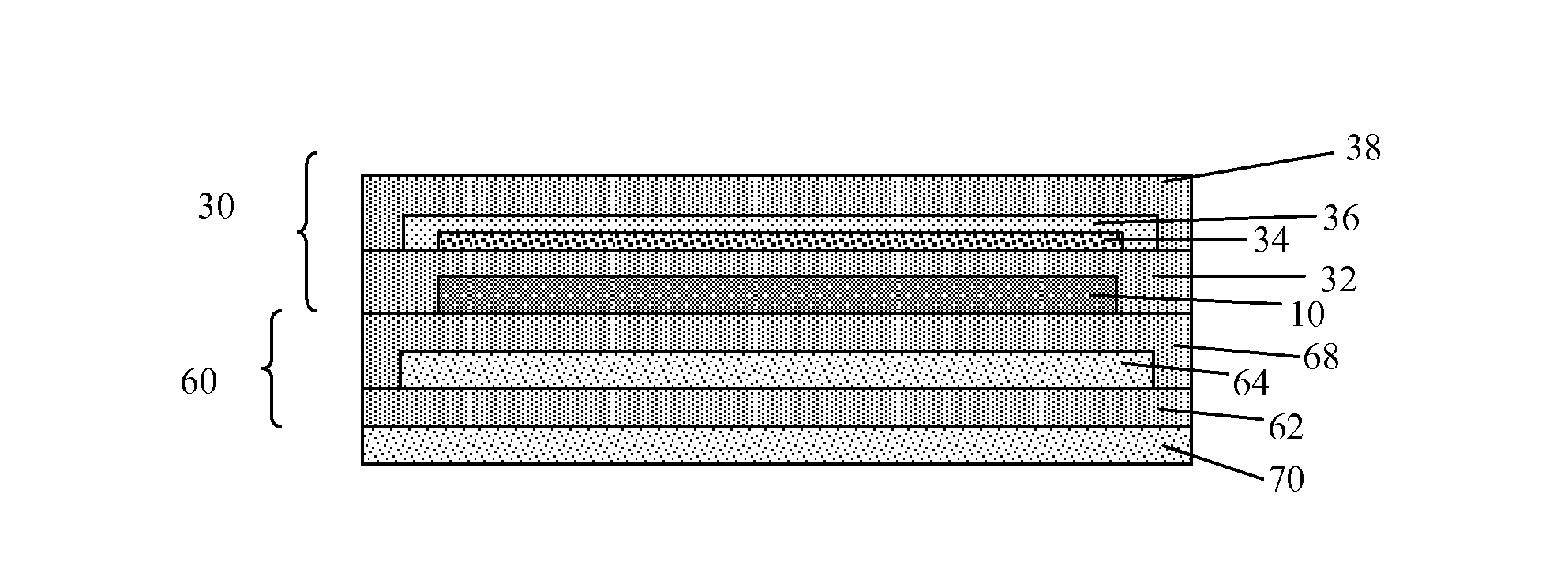
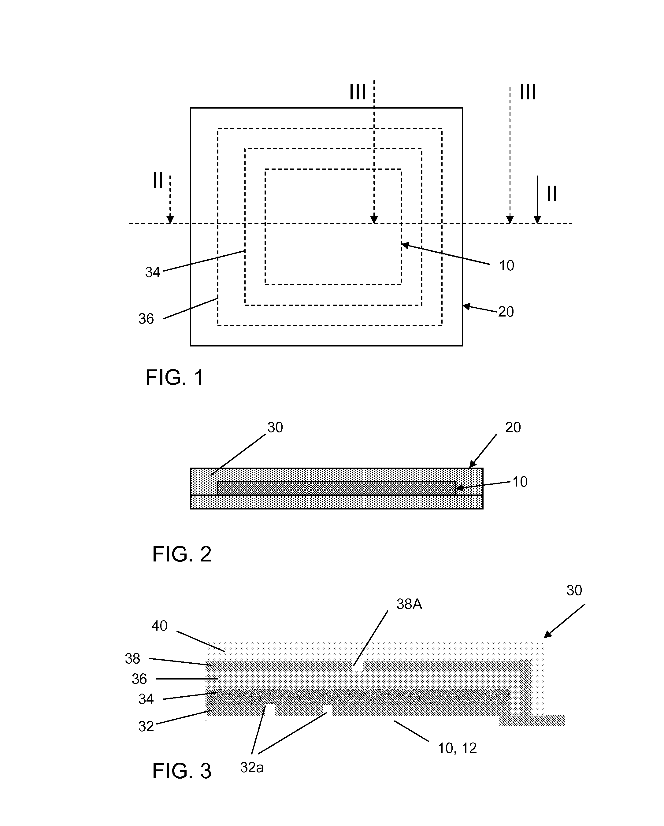
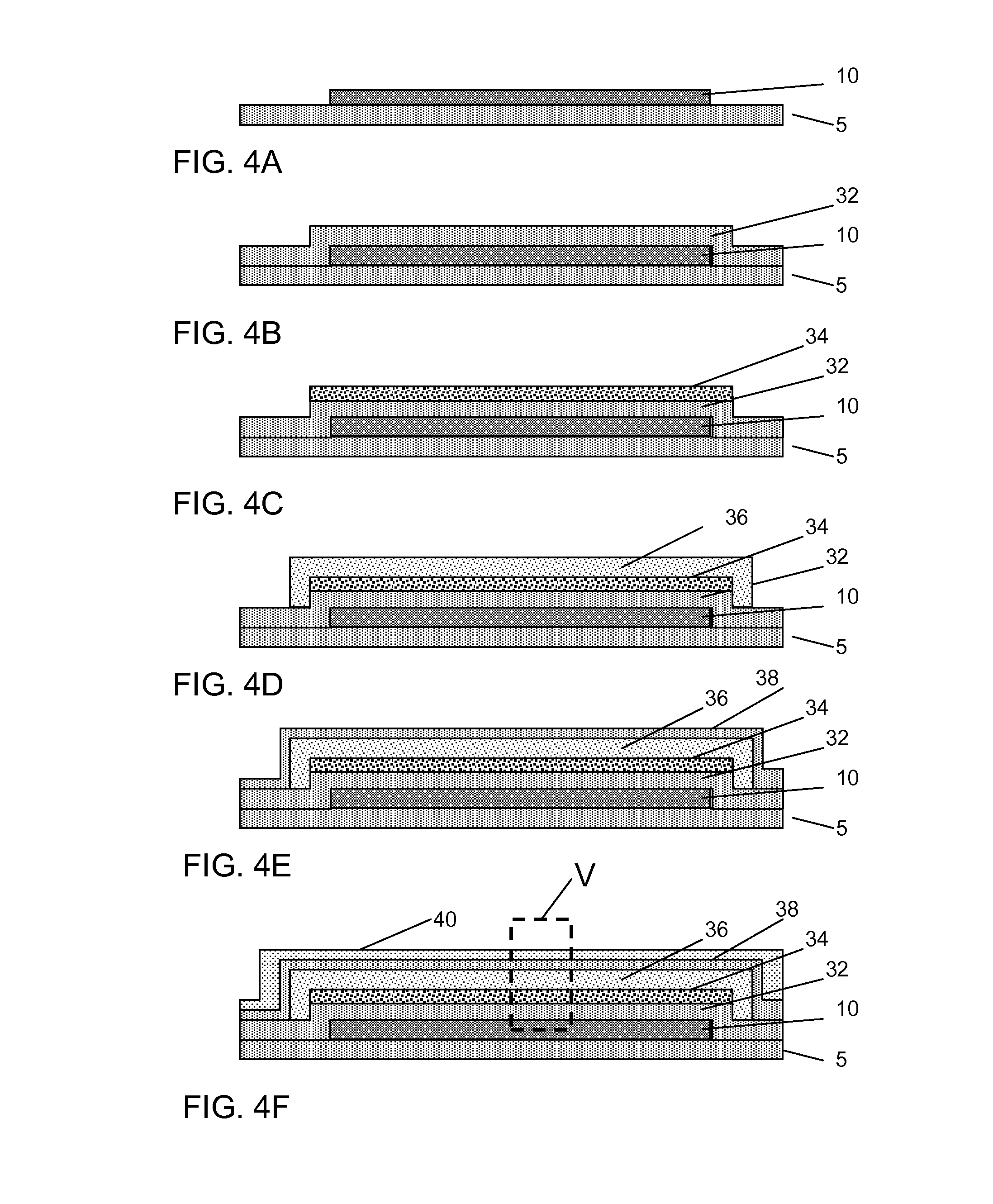
[0103]The invention is described more fully hereinafter with reference to the accompanying drawings, in which embodiments of the invention are shown. This invention may, however, be embodied in many different forms and should not be construed as limited to the embodiments set forth herein. Rather, these embodiments are provided so that this disclosure will be thorough and complete, and will fully convey the scope of the invention to those skilled in the art. In the drawings, the size and relative sizes of layers and regions may be exaggerated for c...


PUM

PropertyMeasurementUnit
thicknessaaaaaaaaaa
thicknessaaaaaaaaaa
thicknessaaaaaaaaaa

Abstract

An organic opto-electric device is disclosed comprising an opto-electric element and a protective enclosure for protecting the opto-electric element against atmospheric substances. The protective enclosure comprises a multi-layered protective layer in which a first inorganic layer, a first organic layer comprising a getter, a second organic layer free from getter material and a second inorganic layer are stacked in the order named, wherein the first and the second inorganic layer encapsulate the first and the second organic layer. The getter is distributed in the first organic layer a nanometer sized particles and the second organic layer has a thickness of at least 10 μm.

Description

BACKGROUND[0001]1. Field of the Invention[0002]The present invention relates to a multilayered protective layer.[0003]The present invention further relates to an organic opto-electric device.[0004]The present invention further relates to a method of manufacturing a multilayered protective layer.[0005]The present invention further relates to a method of manufacturing an organic opto-electric device.[0006]2. Related Art[0007]Exposure of moisture sensitive devices such as organic LEDs (both small molecule and polymer based), OPV, CI(G)S solar cells, to the ambient atmosphere results in loss of performance of the device. In the case of OLEDs, ingress of water or of other oxidising materials can lead to degradation of the active organic layers leading to loss of efficiency or to oxidation of the cathode leading to local failure of the device.[0008]Water ingress can come from two sides, from the anode side or the cathode side. Current state-of-the-art OLEDs are protected from water ingres...

Claims


Application Information

Patent Timeline
Patent Type & Authority Applications(United States)
IPC IPC(8): H01L51/52H01L51/56
CPCH01L51/56H01L51/5253G03F7/027G03F7/038Y02E10/549Y02P70/50H10K30/88H10K50/846H10K50/8445H10K2102/331G03F7/00H10K50/844H10K2102/351H10K71/00
Inventor VAN DE WEIJER, PETERVAN MOL, ANTONIUS MARIA BERNARDUSGALAND, EMILIEFRANTZ, RICHARDKOTZEV, DIMITER LUBOMIROV
Owner NEDERLANDSE ORG VOOR TOEGEPAST-NATUURWETENSCHAPPELIJK ONDERZOEK (TNO)
Why Eureka
Try Eureka