Gate Recessed FDSOI Transistor with Sandwich of Active and Etch Control Layers

a technology of active and etch control layers and transistors, which is applied in the manufacture of metaloxidesemiconductor field effect transistors, and can solve the problems of long time-consuming and laborious, step change in drain current, and un-depleted doping of mos transistors

Active Publication Date: 2014-01-30
SEMIWISE
View PDF6 Cites 16 Cited by
  • Summary
  • Abstract
  • Description
  • Claims
  • Application Information

AI Technical Summary

Problems solved by technology

MOS transistors have long been troubled by the adverse effects of their underlying substrates, like parasitic capacitance and area-consuming isolation.
The un-depleted doped region beneath the gate of a PD SOI transistor proved to have its own disadvantages, largely caused by its tendency to charge and discharge resulting in step changes in the drain current.
These deviations are devastating when billions of transistors are integrated into a single integrated circuit chip.
Layers in the sub-10 nm thickness ranges present manufacturing challenges, and the very thin layers affect performance because the parasitic series resistance in sources and drains cuts down on the transistors' gain figures.
Within the current FDSOI practice there remain problems associated with low and variable access conductance beneath the gate spacers and with thickness control of the active layer.

Method used


Image

  • Gate Recessed FDSOI Transistor with Sandwich of Active and Etch Control Layers
  • Gate Recessed FDSOI Transistor with Sandwich of Active and Etch Control Layers
  • Gate Recessed FDSOI Transistor with Sandwich of Active and Etch Control Layers

Examples


Embodiment Construction

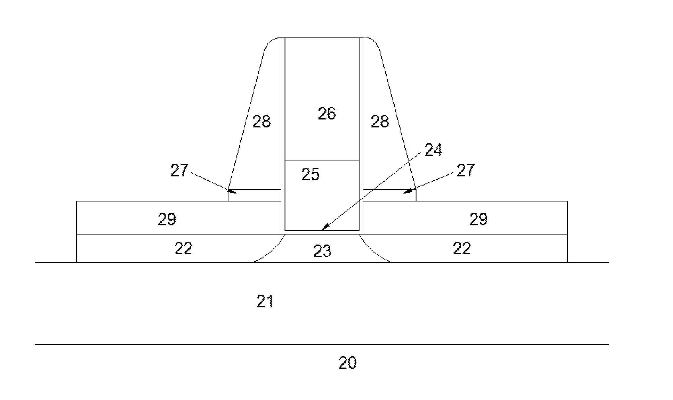
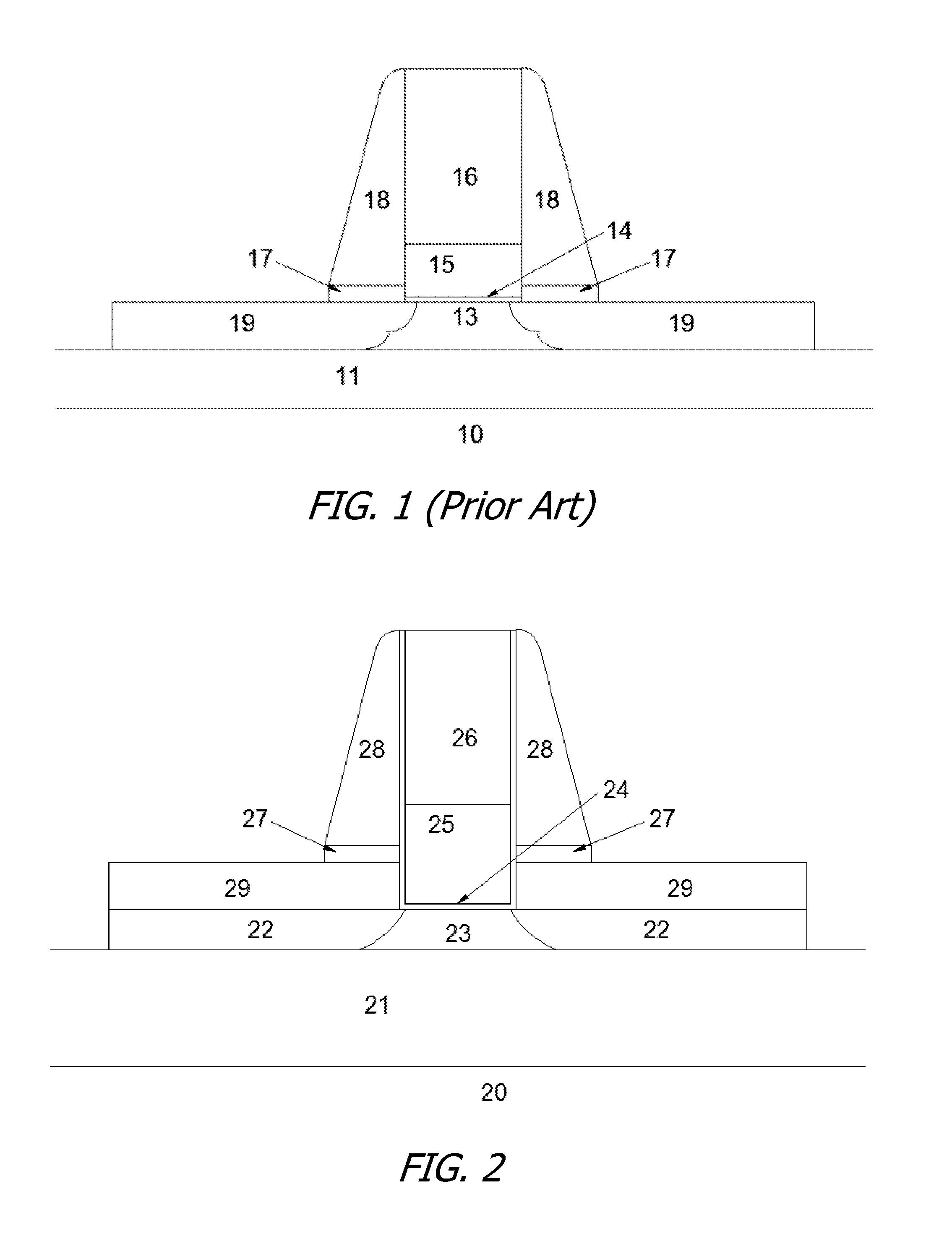
[0017]The structure and the fabrication methods herein implement a fully depleted, recessed gate silicon-on-insulator (SOI) transistor with reduced access resistance, reduced on-current variability, and strain-increased performance. This transistor is based on an SOI substrate that has an epitaxially grown sandwich of SiGe and Si layers that are incorporated in the sources and drains of the transistors. Assuming a metal gate last complementary metal-oxide semiconductor (CMOS) technology and using the sidewall spacers as a hard mask, a recess under the sacrificial gate reaching all the way through the SiGe layer is created, and the high-K gate stack and metal gate are formed within that recess. The remaining Si region, having a precisely controlled thickness, is the fully depleted channel.

[0018]Embodiments of the invention provide for an improved, fully depleted SOI transistor based on a starting substrate having two thin, single crystal layers, one being silicon and the other silico...


PUM


Abstract

The structure and the fabrication methods herein implement a fully depleted, recessed gate silicon-on-insulator (SOI) transistor with reduced access resistance, reduced on-current variability, and strain-increased performance. This transistor is based on an SOI substrate that has an epitaxially grown sandwich of SiGe and Si layers that are incorporated in the sources and drains of the transistors. Assuming a metal gate last complementary metal-oxide semiconductor (CMOS) technology and using the sidewall spacers as a hard mask, a recess under the sacrificial gate reaching all the way through the SiGe layer is created, and the high-K gate stack and metal gate are formed within that recess. The remaining Si region, having a precisely controlled thickness, is the fully depleted channel.

Description

CROSS-REFERENCE TO RELATED APPLICATIONS[0001]This application claims the benefit of U.S. Provisional Patent Application No. 61 / 676,936 filed Jul. 28, 2012.BACKGROUND OF THE INVENTION[0002]1. Field of the Invention[0003]The present invention generally relates to the manufacturing of metal-oxide-semiconductor field effect transistors (MOSFETs), and more particularly to fully depleted channel transistors fabricated in thin silicon films over a buried insulating layer with improved source drain characteristics, excellent electrostatic integrity and reduced statistical variability.[0004]2. Prior Art[0005]MOS transistors have long been troubled by the adverse effects of their underlying substrates, like parasitic capacitance and area-consuming isolation. In the earliest days of integrated circuit technology, the use of a thin film of silicon on a sapphire substrate was proposed as a solution to these problems. RCA Laboratories was an early proponent of this technology, as in Meyer, J. E.;...

Claims


Application Information

Patent Timeline
Patent Type & Authority Applications(United States)
IPC IPC(8): H01L29/78H01L29/66
CPCH01L29/66666H01L29/78H01L29/7848H01L29/78684
Inventor ASENOV, ASEN
Owner SEMIWISE
Why Eureka
Try Eureka