Organic Light-Emitting Diode

a light-emitting diode and organic technology, applied in the field of flat panel display, can solve the problems of inability to effect infrared display, high manufacturing cost, complicated operation, etc., and achieve the effect of simple structure and easy realization

Inactive Publication Date: 2014-02-06
SHENZHEN CHINA STAR OPTOELECTRONICS TECH CO LTD
View PDF5 Cites 19 Cited by
  • Summary
  • Abstract
  • Description
  • Claims
  • Application Information

AI Technical Summary

Benefits of technology

[0010]An object of the present invention is to provide an organic light-emitting diode, which features bot

Problems solved by technology

Commonly used infrared generators include xenon lamps, heated objects, or laser devices, but they cannot effect infrared displaying.
The drawback of the inorganic infrared semiconductor substance is that the manufacture cost is high, the operation is complicated, and is incapable of forming a thin film on a substrate of polycrystalline,

Method used


Image

  • Organic Light-Emitting Diode
  • Organic Light-Emitting Diode
  • Organic Light-Emitting Diode

Examples


Embodiment Construction

[0039]To further expound the technical solution adopted in the present invention and the advantages thereof, a detailed description is given to a preferred embodiment of the present invention and the attached drawings.

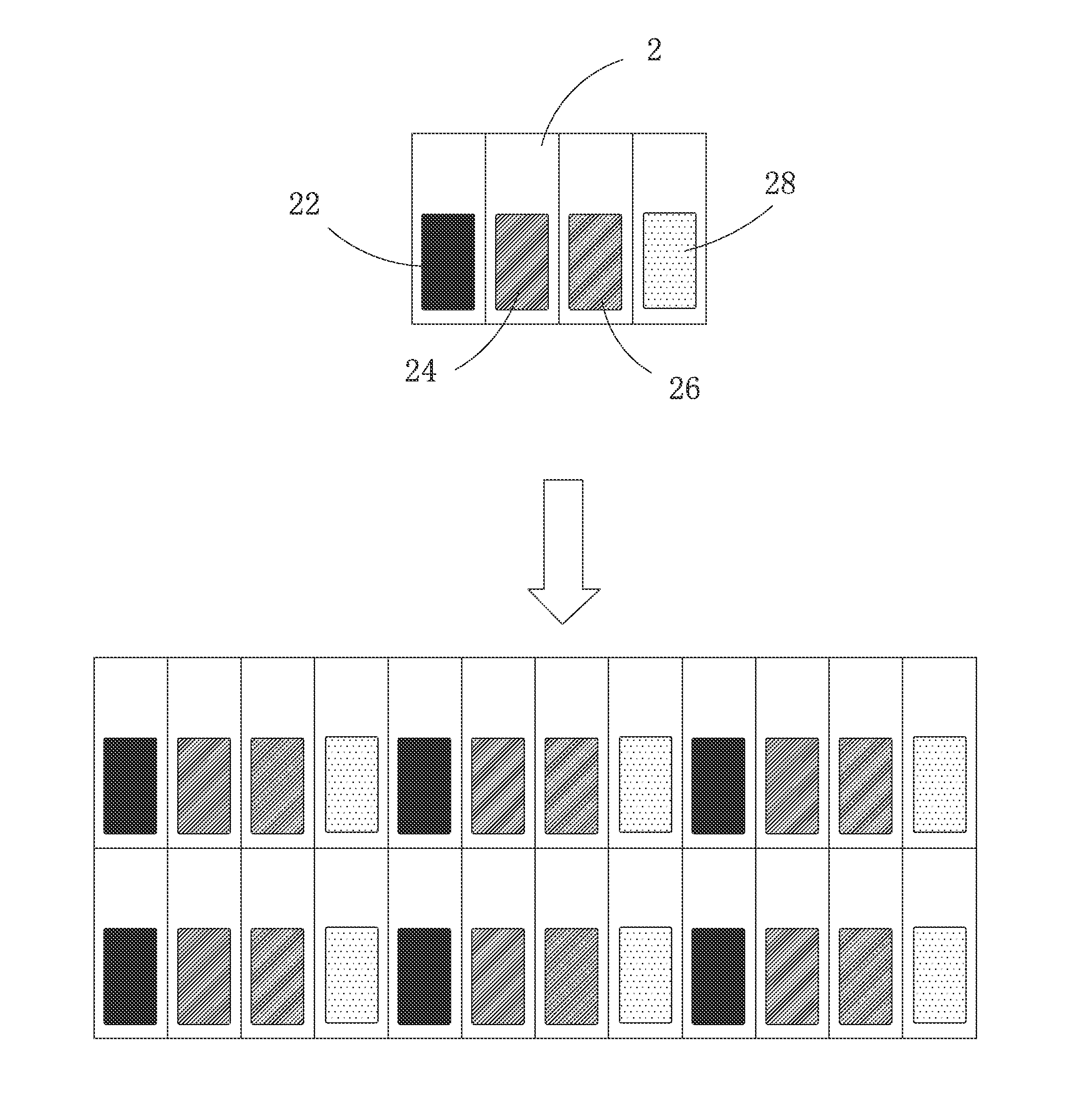
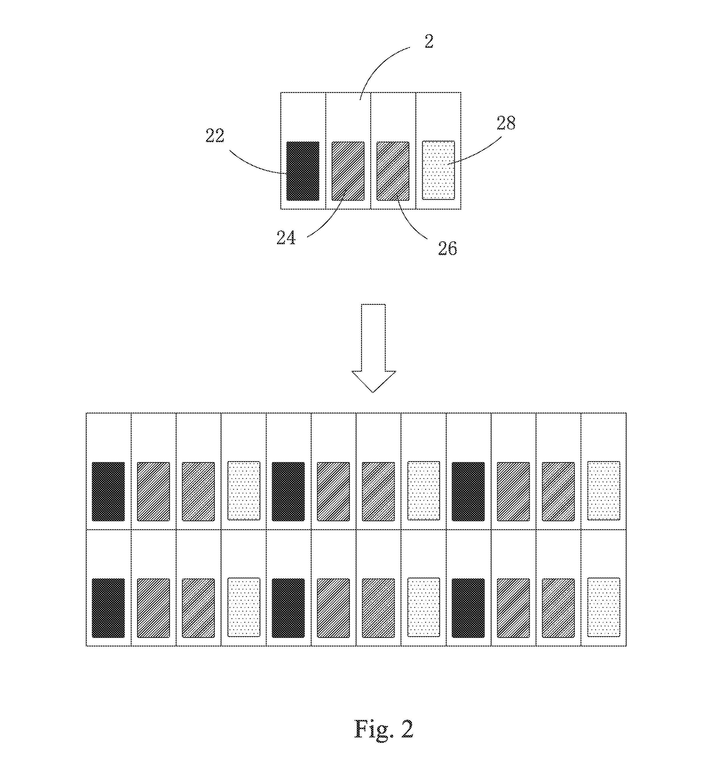
[0040]Referring to FIGS. 2 and 3, the present invention provides an organic light-emitting diode (OLED), which comprises: a light-transmitting substrate, an anode formed on the light-transmitting substrate, a hole transport layer formed on the anode, a light-emitting layer formed on the hole transport layer, an electron transport layer formed on the light-emitting layer, and a cathode formed on the electron transport layer (all being not shown).

[0041]The light-emitting layer comprises a plurality of pixel units 2. Each pixel unit 2 comprises red, green, blue, and infrared sub-pixel points 22, 24, 26, 28. The red, green, blue, and infrared sub-pixel points 22, 24, 26, 28 are all driven by thin-film transistors 4. In the instant embodiment, the red, green, blue, and infr...


PUM


Abstract

The present invention relates to an organic light-emitting diode, which includes: a light-transmitting substrate, an anode formed on the light-transmitting substrate, a hole transport layer formed on the anode, a light-emitting layer formed on the hole transport layer, an electron transport layer formed on the light-emitting layer, and a cathode formed on the electron transport layer. The light-emitting layer includes a plurality of pixel units, each of which includes red, green, blue, and infrared sub-pixel points. The red, green, blue, and infrared sub-pixel points are driven by thin-film transistors. The organic light-emitting diode of the present invention combines color displaying and infrared displaying in a single component and realizes switchability between color displaying and infrared displaying in the same component. The organic light-emitting diode greatly reduces the manufacture cost, shows wide applicability, and facilitates popularization

Description

BACKGROUND OF THE INVENTION[0001]1. Field of the Invention[0002]The present invention relates to the field of flat panel display, and in particular to an organic light-emitting diode (OLED).[0003]2. The Related Arts[0004]Infrared waveband is an important electromagnetic wave band for military and civil applications and has a wavelength range of 0.78-1,000 μm. Infrared light is commonly used in heating, physiotherapy, night vision, communication, navigation, plant growing, and animal farming. Applications of infrared light that are commonly seen in regular living include high-temperature sterilization, infrared light night vision device, surveillance device, infrared port of mobile phone, card key of hotel room, remote controls of automobile and television set, infrared sensing for wash basin, and infrared sensing door. Further, window wavelengths of optic fiber communication, including 850 nm, 1,130 nm, and 1,550 nm, are all located in the infrared waveband. Further, the infrared wa...

Claims


Application Information

Patent Timeline
IPC IPC(8): H01L51/00
CPCH01L51/0084H01L51/0078H10K59/351H10K85/351H10K85/311H10K85/341
Inventor LIU, YAWEIWU, YUANCHUN
Owner SHENZHEN CHINA STAR OPTOELECTRONICS TECH CO LTD
Why Eureka
Try Eureka