Organic el element and manufacturing method thereof, and metal oxide film forming method
a technology of organic el elements and metal oxides, which is applied in the direction of solid-state devices, semiconductor devices, thermoelectric devices, etc., can solve the problems of deterioration, low work function metals, and many organic materials, and achieve excellent electron conduction, high transmittance, and stable air
- Summary
- Abstract
- Description
- Claims
- Application Information
AI Technical Summary
Benefits of technology
Problems solved by technology
Method used
Image
Examples
embodiment 1
[0047](Structure of Organic EL Element)
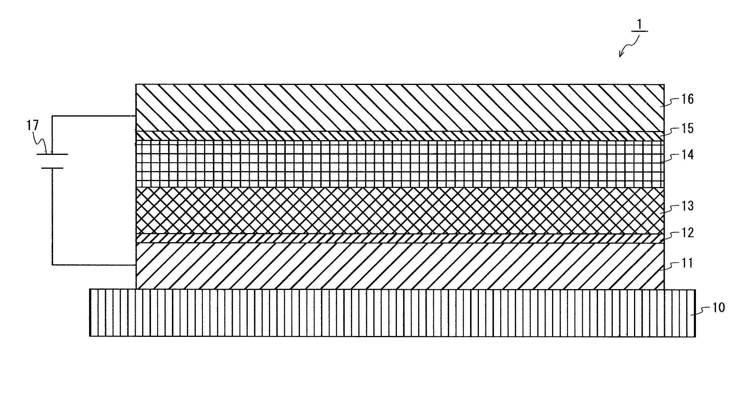
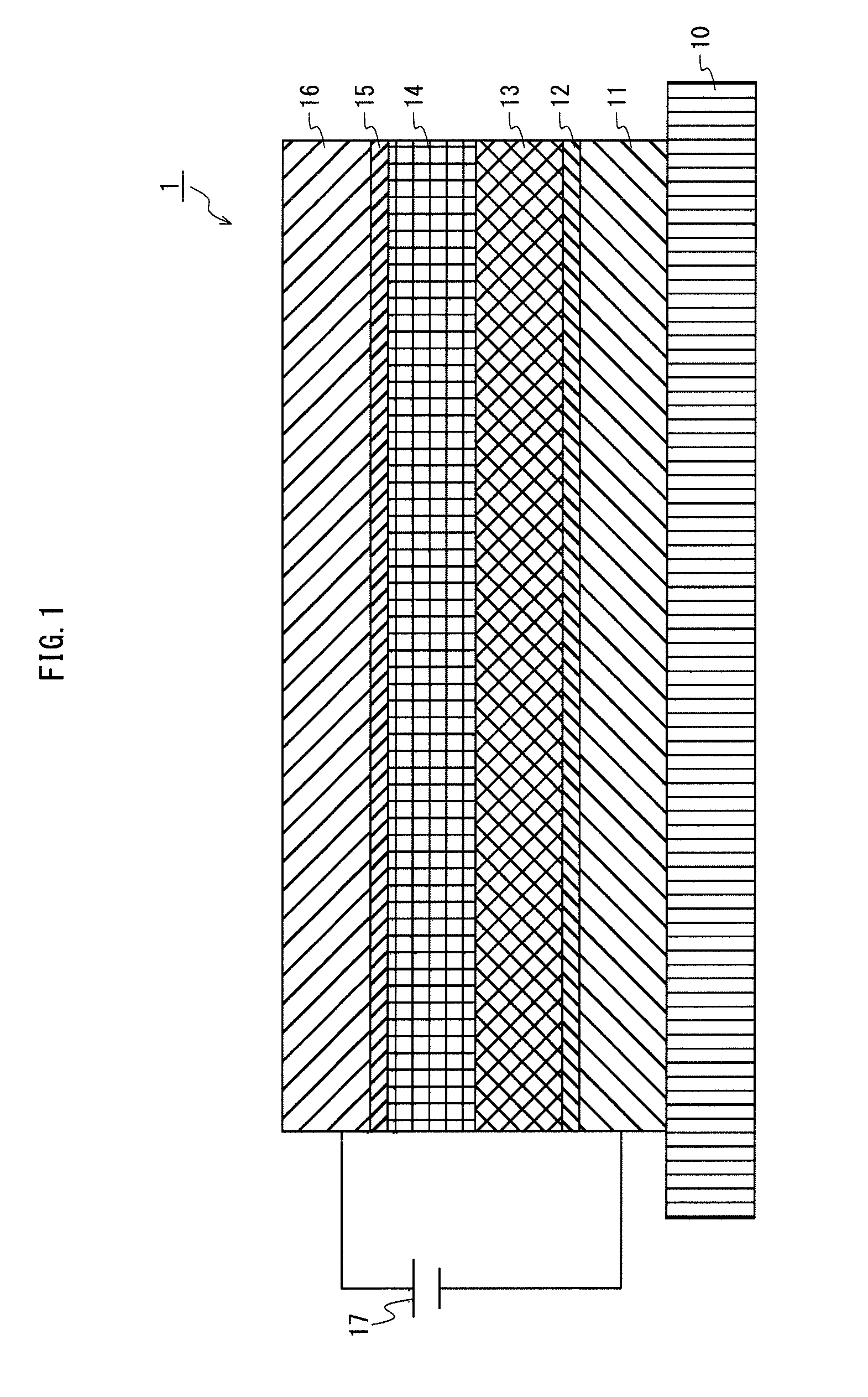
[0048]FIG. 1 is a schematic cross-sectional view illustrating a part of the structure of an organic EL element 1 in Embodiment 1.
[0049]As illustrated in FIG. 1, the organic EL element 1 in the present embodiment has a structure where a laminate of an electron injection layer 12 and functional layers having predetermined functions (in this example, a light-emitting layer 13, a hole transport layer 14 and a hole injection layer 15) is inserted between a cathode 11 and an anode 16 that make an electrode pair.
[0050]More specifically, as illustrated in FIG. 1, the organic EL element 1 is formed by laminating the cathode 11, electron injection layer 12, light-emitting layer 13, hole transport layer 14, hole injection layer 15, and anode 16 on a main surface of a substrate 10 in the stated order. The anode 16 and the cathode 11 are connected with a power supply 17 such that power is supplied to the organic EL element 1 from an external source.
[0051](C...
embodiment 2
[0122](Structure of Organic EL Element)
[0123]FIG. 7 is a schematic cross-sectional view illustrating a part of the structure of an organic EL element 2 in Embodiment 2.
[0124]The organic EL element 2 is a solution-processed organic EL element that is manufactured by coating the electron injection layer, light-emitting layer and buffer layer by the wet process, and has a structure where a laminate of an electron injection layer 22 and functional layers having predetermined functions (in this example, a hole injection layer 25, a buffer layer 24, and a light-emitting layer 23) is inserted between a cathode 21 and an anode 26 that make an electrode pair.
[0125]More specifically, as illustrated in FIG. 7, the organic EL element 2 is formed by laminating the anode 26, hole injection layer 25, buffer layer 24, light-emitting layer 23, electron injection layer 22, and cathode 21 on a main surface of a substrate 20 in the stated order.
[0126](Anode)
[0127]The cathode 26 is made of, for example,...
PUM
 Abstract
Description
Claims
Application Information


