Substrate processing device and substrate processing method for carrying out chemical treatment for substrate

a substrate processing and processing method technology, applied in semiconductor/solid-state device manufacturing, basic electric elements, electric devices, etc., can solve the problems of reducing the yield or trouble of the substrate processing device itself, increasing the amount of processing liquid and the processing time required for the etching of the peripheral edge part, and reducing the etching rate. , to achieve the effect of suppressing the amount of processing liquid and the time required, suppressing the etching rate, and suppressing the etching width

Active Publication Date: 2014-02-20
DAINIPPON SCREEN MTG CO LTD
View PDF16 Cites 17 Cited by
  • Summary
  • Abstract
  • Description
  • Claims
  • Application Information

AI Technical Summary

Benefits of technology

[0015]The processing liquid is supplied to the peripheral edge part of the substrate heated by injecting the heating steam so that the chemical treatment for the peripheral edge part is carried out. Accordingly, it is possible to suppress reduction in a temperature of the peripheral edge part of the substrate by the rotation. Consequently, a change in the chemical activity of the processing liquid is also reduced and an amount of consumption of the processing liquid and a time required for processing are suppressed. The gas is injected from above the substrate toward the predetermined injection target region defined within the range surrounded by the rotating track of the peripheral edge part of the substrate in the upper surface of the substrate, to generate, on the substrate, a gas flow which flows from the injection target region toward the peripheral edge part of the substrate. Consequently, it is possible to prevent mist obtained by condensation of the steam or a mist-like processing liquid from adhering onto a non-processed region of the upper surface of the substrate. Therefore, it is possible to supply a sufficient amount of steam for heating the peripheral edge part of the substrate while suppressing deterioration in the non-processed region due to the adhering of the mist.
[0017]The processing liquid is discharged from the processing liquid discharging port of the lower surface processing portion including the opposed surface which is opposed to the substantially entire region of the lower surface of the substrate to be rotated so that the space between the lower surface of the substrate and the opposed surface is brought to the fluid-tight condition with the processing liquid. Therefore, even if the substrate is rotated at a low speed, the processing liquid can be supplied to the entire region of the lower surface of the substrate. Consequently, it is possible to carry out the chemical treatment for the peripheral edge part and the lower surface in the substrate while suppressing a drop in the temperature of the peripheral edge part of the substrate, thereby reducing energy required for heating the peripheral edge part. Moreover, it is possible to suppress wraparound of the processing liquid from the lower surface of the substrate to the peripheral edge part of the upper surface of the substrate by reducing the rotating speed of the substrate. Thus, it is easy to control the processing width of the peripheral edge part.
[0019]The peripheral edge part is heated in the plurality of different positions in the rotating track of the peripheral edge part of the substrate respectively and the processing liquid is supplied to the peripheral edge part from above. Therefore, even in the case where the heating width in the radial direction in the peripheral edge part is small, the temperature of the peripheral edge part can be prevented from being reduced. Even if the amount of the processing liquid is small, it is possible to enhance reactivity of the processing liquid by suppressing reduction in a reaction rate of the processing liquid in the region having a small width which is heated by the heating portion in the peripheral edge part of the upper surface of the substrate. Accordingly, it is possible to reduce the chemical treating width while suppressing deterioration in each of uniformity of the chemical processing width and processing efficiency.
[0023]Therefore, it is an object of the present invention to provide a technique capable of suppressing an amount of consumption of a processing liquid and a time required for processing. Moreover, it is another object of the present invention to provide a technique capable of reducing a chemical treating width (an etching width or the like) while suppressing deterioration in each of uniformity of the chemical treating width and chemical treating efficiency (an etching rate or the like).

Problems solved by technology

In cases where the film is formed on the back surface of the substrate or the peripheral edge part of the upper surface of the substrate, a thin film formed on the peripheral edge part of the upper surface of the substrate may be peeled by contact with another device at a subsequent step to the film forming step, and may cause reduction in yield or a trouble of a substrate processing device itself.
However, the devices disclosed in Japanese Patent Application Laid-Open Nos. 2004-6672 and 2008-47629 have a problem in that the amount of the processing liquid and the processing time which are required for the etching in the peripheral edge part are increased because the temperature of the peripheral edge part is reduced due to the rotation of the substrate, resulting in decrease in the etching rate.
According to the method, although an average etching width can be reduced, uniformity of the etching width is deteriorated, for example, the amount of wraparound of the processing liquid to the peripheral edge part is controlled with difficulty so that a portion to be etched locally and greatly appears.
Furthermore, there is also a problem in that the temperatures of the peripheral edge part and the processing liquid in the peripheral edge part are lowered, resulting in reduction in an etching rate.
However, there is a problem in that the etching rate in the peripheral edge part of the substrate is reduced due to decrease in the amount of the processing liquid and reduction in the temperature of the processing liquid in a pipe due to the decrease.
These are problems which are not limited to the etching using an etchant, but are caused in general processing for carrying out a chemical treatment for a substrate by using a processing liquid having a chemical activity (chemical reactivity) varied depending on a temperature (a processing liquid having a reaction rate increased with a rise in temperature).

Method used


Image

  • Substrate processing device and substrate processing method for carrying out chemical treatment for substrate
  • Substrate processing device and substrate processing method for carrying out chemical treatment for substrate
  • Substrate processing device and substrate processing method for carrying out chemical treatment for substrate

Examples


Embodiment Construction

[0043]A preferred embodiment according to the present invention will be described below with reference to the drawings. Portions having the same structures and functions have the same reference numerals in the drawings, and repetitive description will be omitted in the following explanation. Moreover, each of the drawings is shown schematically, and for example, a size, a positional relationship and the like of an illustrated member in the drawing are not always shown accurately.

Referring to First Preferred Embodiment

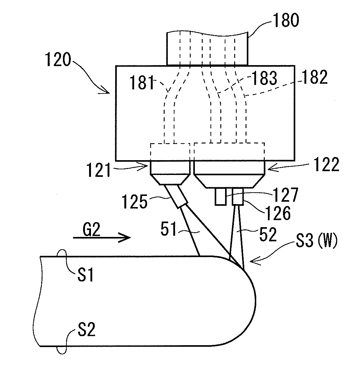
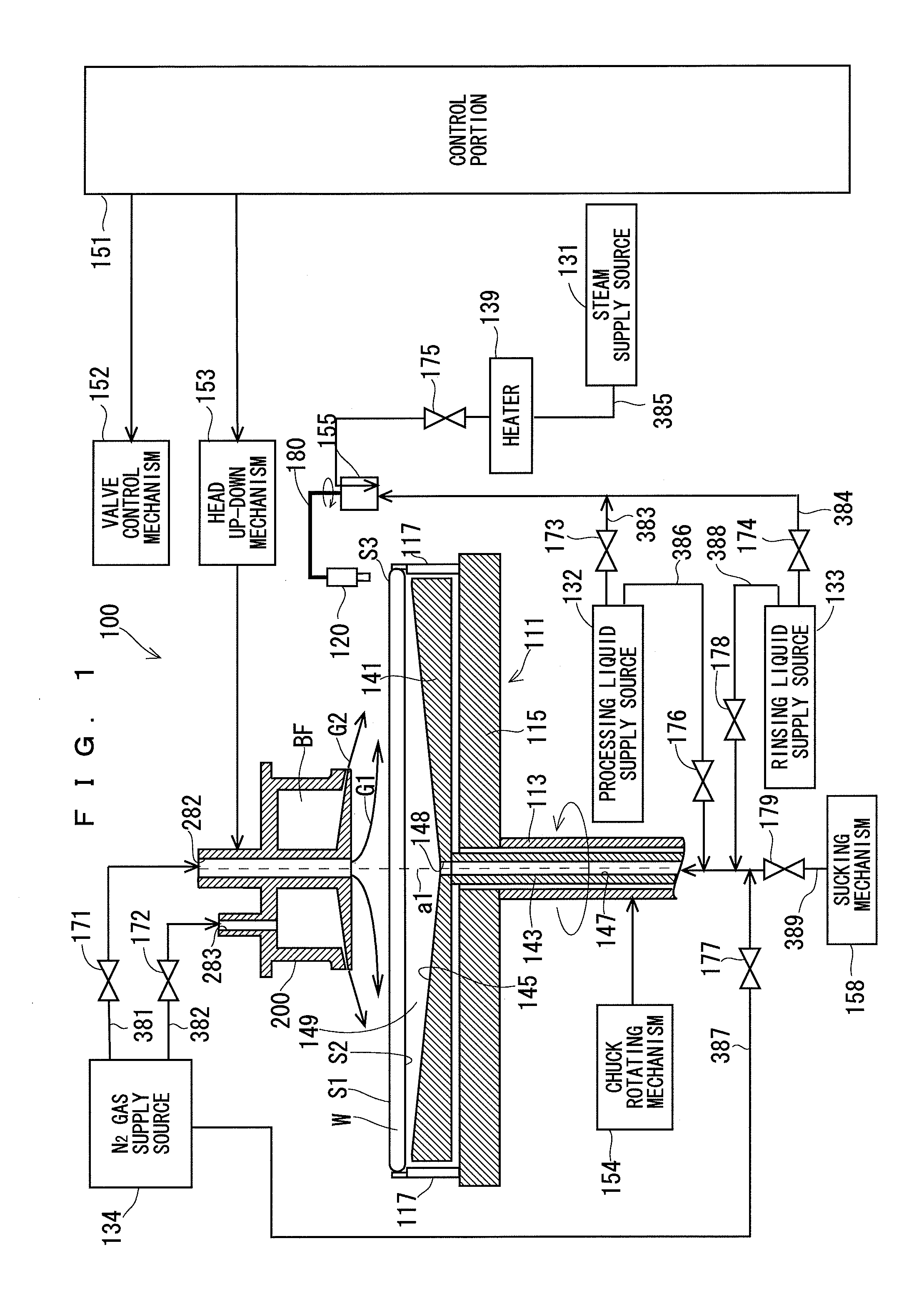
[0044]FIG. 1 is a view schematically showing an example of a schematic structure of a substrate processing device 100 according to a first preferred embodiment. The substrate processing device 100 carries out a chemical treatment for a substrate by using a processing liquid having a chemical activity varied depending on a temperature. More specifically, the substrate processing device 100 performs etching over a peripheral edge part (also referred to as “an upper surfac...


PUM

PropertyMeasurementUnit
diameteraaaaaaaaaa
widthaaaaaaaaaa
temperatureaaaaaaaaaa

Abstract

It is an object to carry out a chemical treatment for a peripheral edge part of a substrate while suppressing an amount of consumption of a processing liquid and a time required for processing. In order to achieve the object, a substrate processing device injects heating steam to a peripheral edge part of a substrate to heat the peripheral edge part when carrying out a chemical treatment for the peripheral edge part of the substrate while rotating the substrate in a substantially horizontal posture. Moreover, the substrate processing device injects a gas from above the substrate toward a predetermined injection target region defined within a range surrounded by a rotating track of the peripheral edge part of the substrate in an upper surface of the substrate, thereby generating, on the substrate, a gas flow which flows from the injection target region toward the peripheral edge part of the substrate.

Description

BACKGROUND OF THE INVENTION[0001]1. Field of the Invention[0002]The present invention relates to a substrate processing device and a substrate processing method for supplying a processing liquid to a substrate to carry out a chemical treatment such as etching while rotating the substrate. The substrate to be processed includes substrates, for example, a semiconductor wafer, a substrate for an optical disk, a substrate for a magnetic disk, a substrate for a magneto-optical disk, a substrate for a photomask, a substrate for a solar cell, and the like.[0003]2. Description of the Background Art[0004]Although a series of processing steps for a substrate such as a semiconductor wafer have a plurality of film forming steps for forming a thin film of a metal, a photoresist or the like on a front surface (“an upper surface”) of the substrate, a film is also formed on a back surface (“a lower surface”) of the substrate or a peripheral edge part of the upper surface of the substrate at the fil...

Claims


Application Information

Patent Timeline
Patent Type & Authority Applications(United States)
IPC IPC(8): H01L21/306H01L21/67
CPCH01L21/6708H01L21/30604H01L21/02087H01L21/0209H01L21/32134H01L21/67028H01L21/67086H01L21/302H01L21/306
Inventor IZUMOTO, KENJISHIBAYAMA, NOBUYUKI
Owner DAINIPPON SCREEN MTG CO LTD
Why Eureka
Try Eureka