Wide gap semiconductor device and method for manufacturing the same

a semiconductor device and wide gap technology, applied in semiconductor devices, diodes, electrical devices, etc., can solve the problems of difficulty in sufficiently lowering the leakage current of schottky diodes, and achieve the effect of less leakage current and efficient heating

Inactive Publication Date: 2014-03-06
SUMITOMO ELECTRIC IND LTD
View PDF0 Cites 8 Cited by
  • Summary
  • Abstract
  • Description
  • Claims
  • Application Information

AI Technical Summary

Benefits of technology

[0017]In the method for manufacturing a wide gap semiconductor device according to the above, preferably, the step of heating the entire Schottky electrode is performed through laser annealing. Thus, the Schottky electrode can efficiently be heated.
[0018]According to the present invention, a wide gap semiconductor device capable of achieving less leakage current and a method for manufacturing the same can be provided.

Problems solved by technology

It has been difficult, however, to sufficiently lower a leakage current in the Schottky diodes described in Japanese Patent Laying-Open No. 2001-85704 and Japanese Patent Laying-Open No. 2009-16603.

Method used


Image

  • Wide gap semiconductor device and method for manufacturing the same
  • Wide gap semiconductor device and method for manufacturing the same
  • Wide gap semiconductor device and method for manufacturing the same

Examples


example

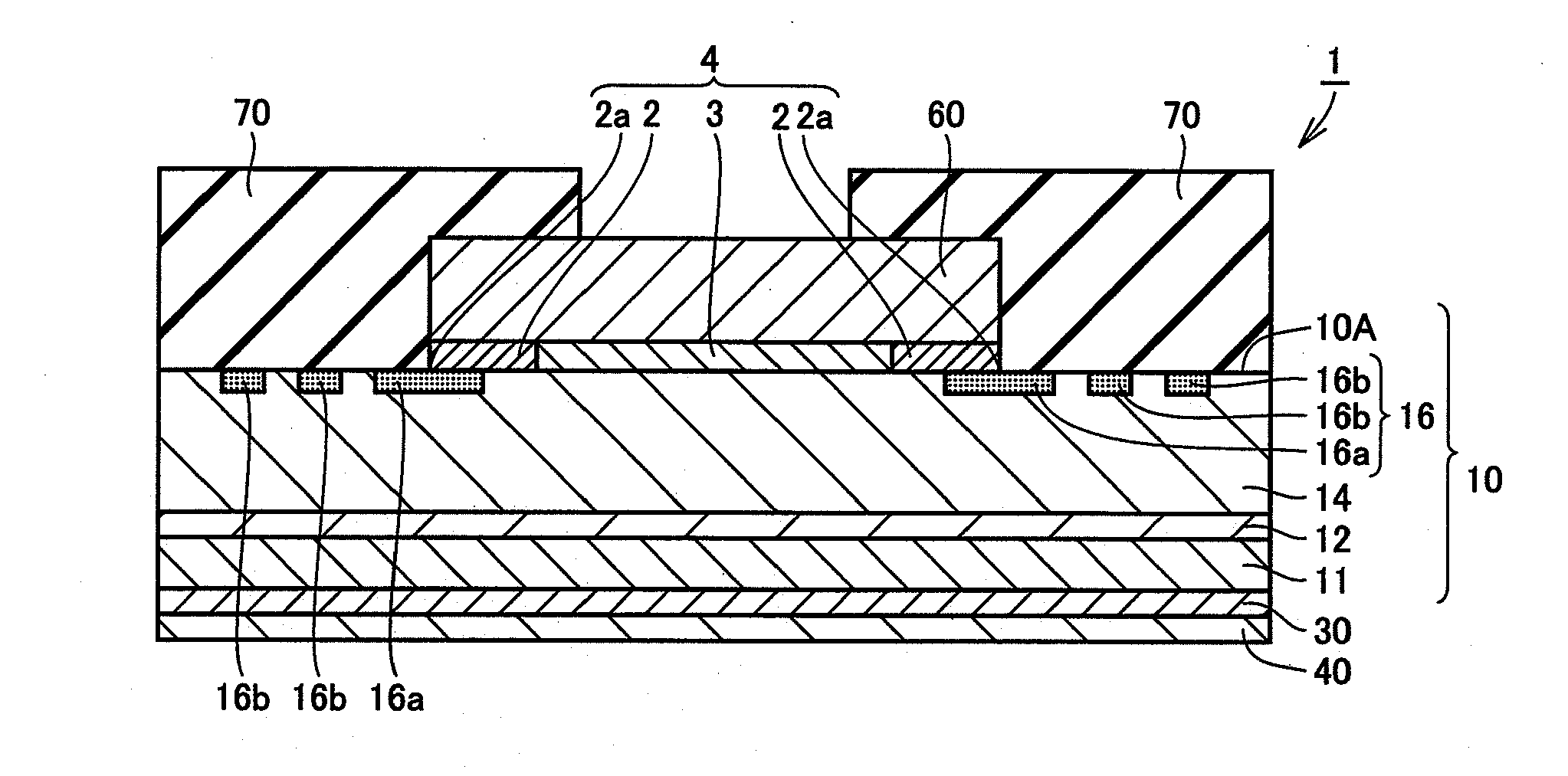
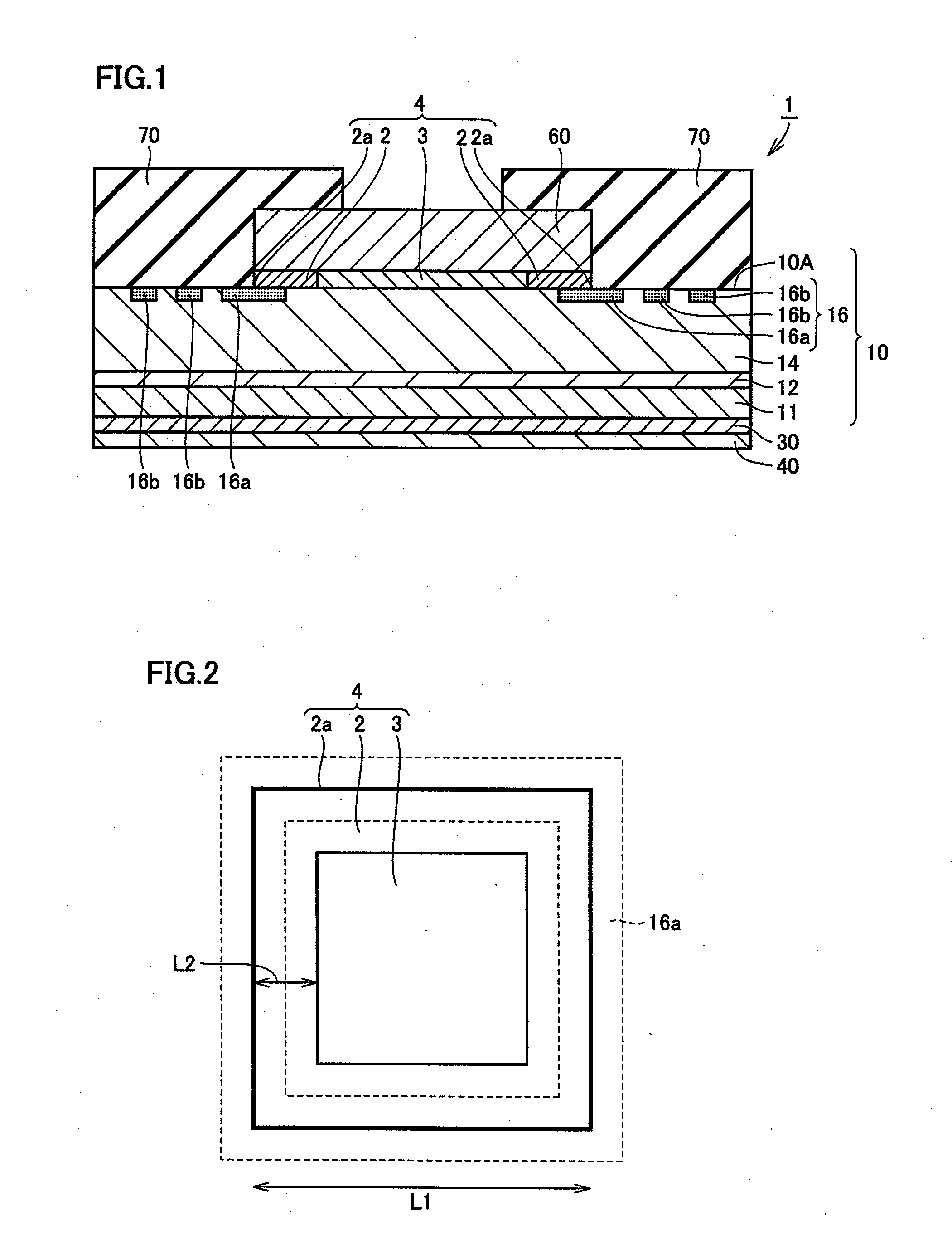
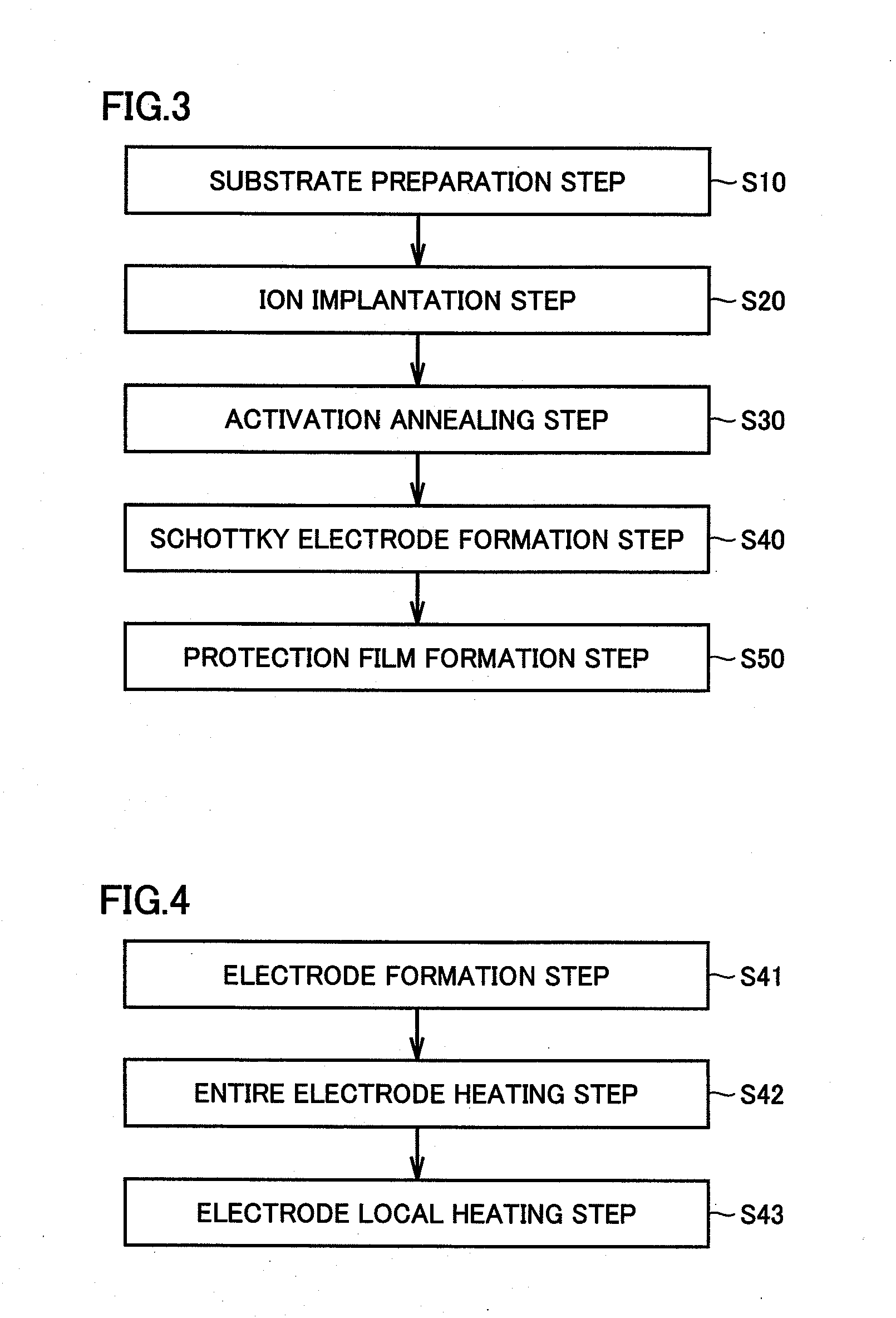
[0062]In the present example, relation between a temperature for annealing a Schottky electrode and a barrier height of a Schottky barrier diode has been investigated. Initially, a Schottky barrier diode as shown in FIG. 9 was manufactured with a method the same as the method described in the first embodiment. Specifically, Schottky electrode 4 was made of titanium. Electric field stop layer 12 was formed on n′ substrate 11 and an n− drift layer was formed on electric field stop layer 12. Ohmic electrode 30 was formed on a side of n+ substrate 11 opposite to electric field stop layer 12. Schottky electrode 4 was heated through laser annealing. A temperature for laser annealing was set to room temperature (As-depo), 300° C., 450° C., 500° C., and 550° C. A time period for annealing was set to 5 minutes in all temperature conditions. As shown in FIG. 10, current density was measured while a voltage for 5 types of Schottky barrier diodes different in annealing temperature was varied fr...


PUM


Abstract

A wide gap semiconductor device has a substrate and a Schottky electrode. The substrate is made of a wide gap semiconductor material and has a first conductivity type. The Schottky electrode is arranged on the substrate to be in contact therewith and is made of a single material. The Schottky electrode includes a first region having a first barrier height and a second region having a second barrier height higher than the first barrier height. The second region includes an outer peripheral portion of the Schottky electrode. Thus, a wide gap semiconductor device capable of achieving less leakage current and a method for manufacturing the same can be provided.

Description

BACKGROUND OF THE INVENTION[0001]1. Field of the Invention[0002]The present invention relates to a wide gap semiconductor device and a method for manufacturing the same and more particularly to a wide gap semiconductor device capable of achieving a suppressed leakage current and a method for manufacturing the same.[0003]2. Description of the Background Art[0004]Such a semiconductor device as a Schottky barrier diode (SBD) or a junction barrier Schottky diode (JBS) has a structure that a Schottky electrode is formed on a substrate. Since a Schottky barrier diode is small in difference in work function between a metal and a semiconductor employed as electrode materials, a leakage current at the time of application of a reverse voltage tends to be higher than in a PN diode. Therefore, various structures for lowering a leakage current have been proposed.[0005]For example, Japanese Patent Laying-Open No. 2001-85704 discloses a silicon carbide Schottky diode in which a p+ guard ring regio...

Claims


Application Information

Patent Timeline
Patent Type & Authority Applications(United States)
IPC IPC(8): H01L29/872H01L29/66
CPCH01L29/66143H01L29/872H01L21/0495H01L29/0619H01L29/1602H01L29/1608H01L29/2003H01L29/47H01L29/475H01L29/66022H01L29/6603H01L29/6606H01L29/66212
Inventor WADA, KEIJIKANBARA, KENJI
Owner SUMITOMO ELECTRIC IND LTD
Why Eureka
Try Eureka